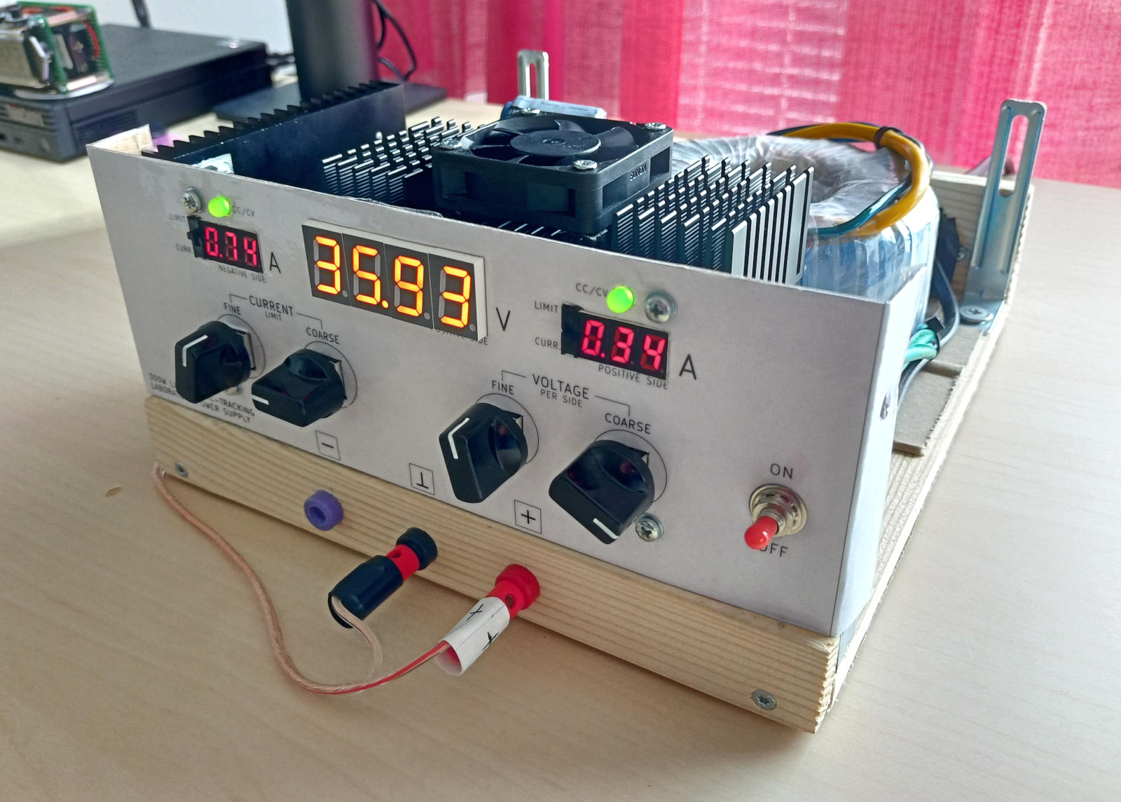
300W Linear Dual-Tracking Lab Supply
So what to do with all the newly acquired experience of creating finely detailed circuit boards, SMT and all?
Something I badly needed: a bench-top power supply to facilitate further lab work. Able to output a stable, symmetrical supply voltage (for feeding op-amp circuits, push-pull power amplifiers, etc.) and provide plenty of current. Having settable current limits (protecting both itself and the circuit being fed) and precise digital meters of everything (voltage and currents on both sides) is a bonus.
It took me several months to design and build this instrument from scratch. Below is a write-up of the journey as well as a presentation of the end result.
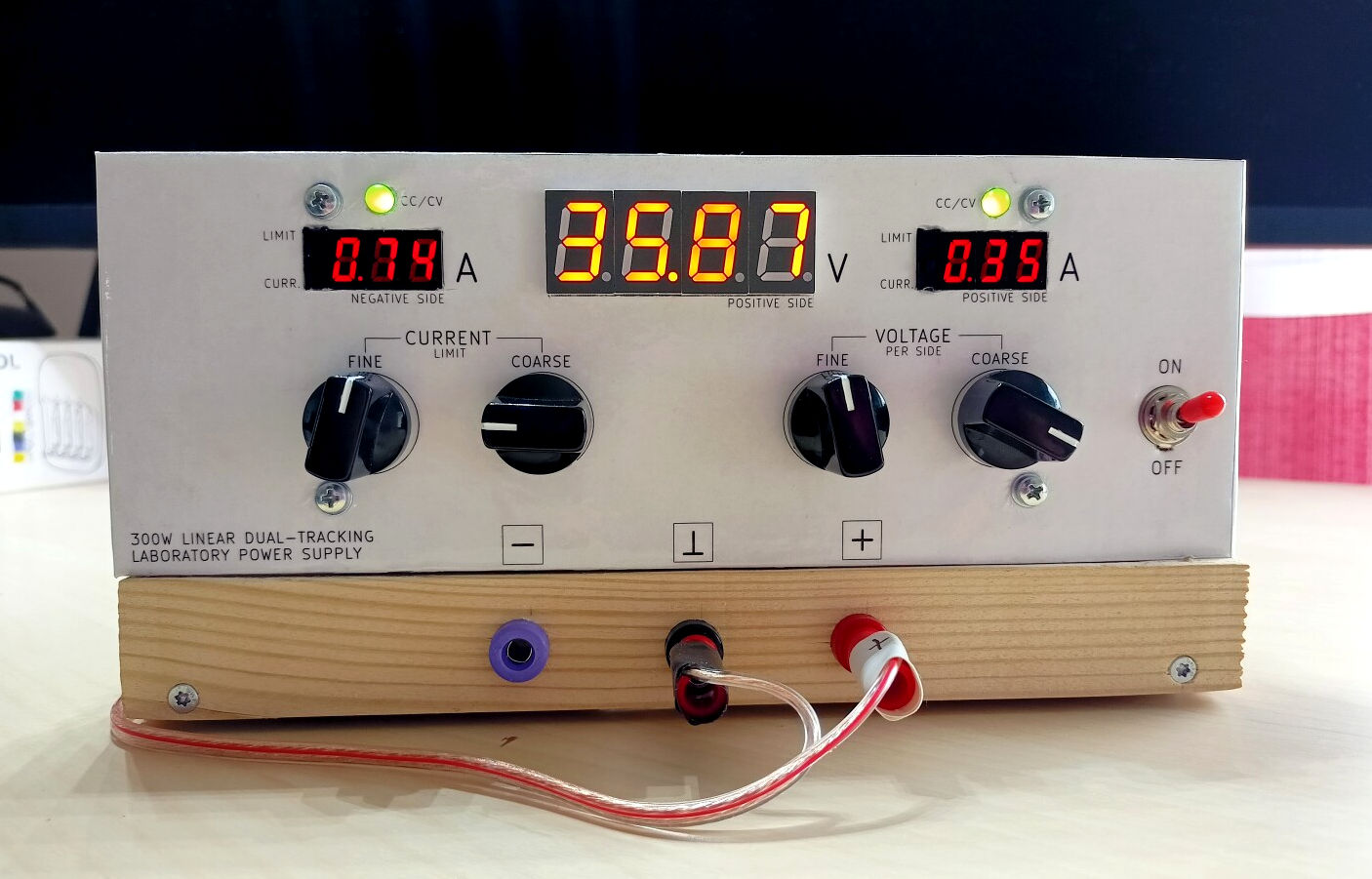
Instrument front panel (click to enlarge)
Update: some very valid comments criticising this design in the discussion – thanks all! I am aware of several design flaws (and will point them out below). Please keep in mind that this is not a professional product. Take this article as entertainment but do not copy it for yourself; there are better designs to steal from!
Features
- Output voltage between ±0V and ±38V
- Current limit between ±0A and ±5A
- Coarse and fine adjustment of output voltage and current limit
- 4-digit voltage readout with 10mV resolution
- 3-digit current readouts with 10mA resolution
- Per-side CC/CV mode indicator (CC: red, CV: green)
- Per-side switches to toggle current display between set limit and measured value
Circuit overview
This is going to be a very old school, linear, transistor-regulated power supply built on a conventional circuit topology. That is, we are not building a switch-mode power supply (at least not yet). Also, we are not building our circuit on LM317 or similar all-in-one adjustable regulator ICs. The former because we want to target a simple enough circuit with some real chance to succeed with developing it. And the latter because, well, we want higher output current than any of those can provide!
Okay, so within this framework, what would be the most important component of our instrument?
You guessed right: yes, it’s the mains transformer. And the best kind you can use is a toroidal transformer. Here are three I had lifted from earlier, dead projects (mainly audio amplifiers) from a different era of about 25 years ago:
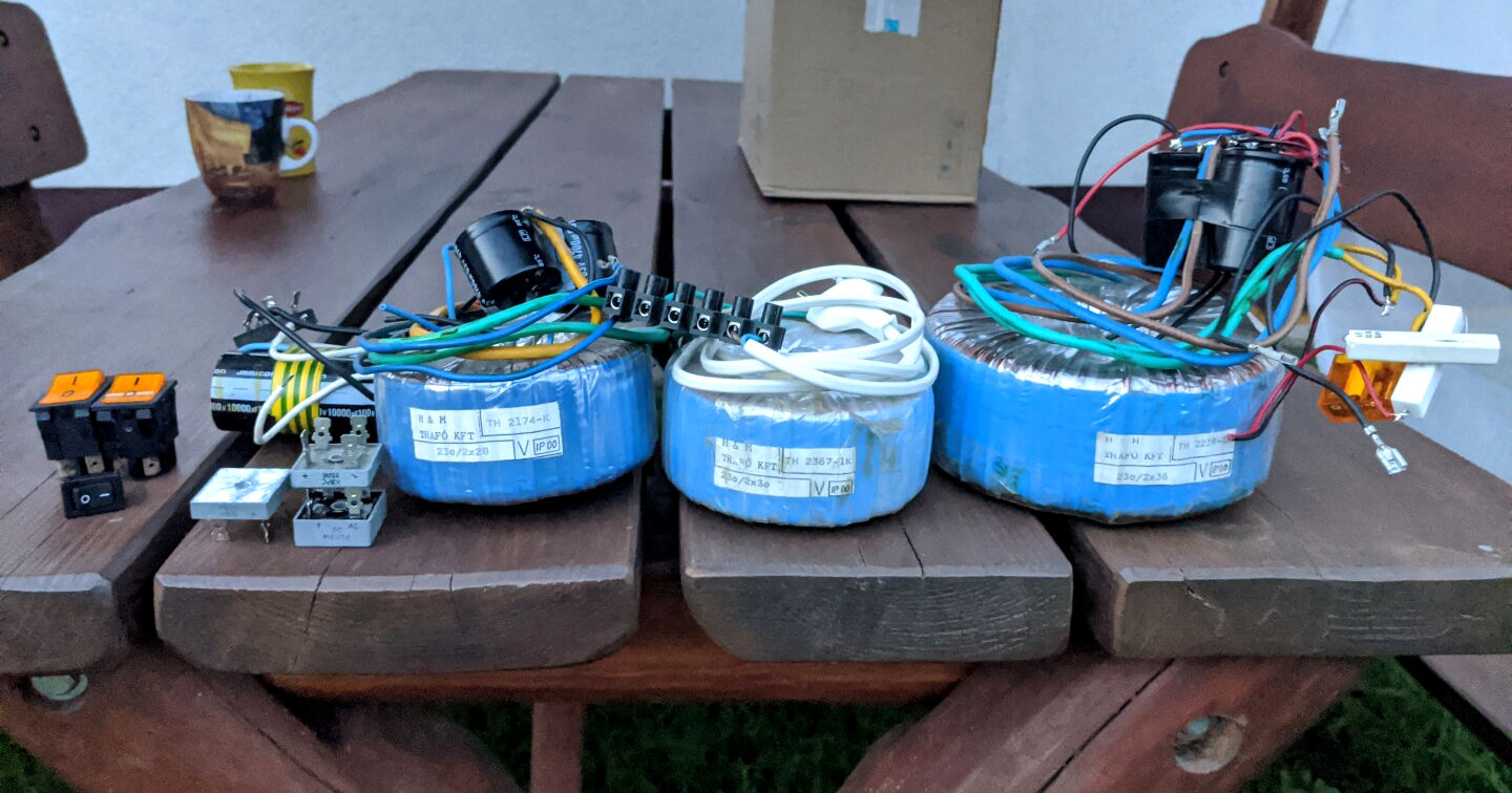
My historical baggage of toroids with associated cruft (click to enlarge)
The mains transformer has a very direct influence on the output voltage, current, and power capacity of our instrument, as well as the output topology (single, dual, etc). It is also the single most expensive component. Thankfully, toroids have excellent characteristics overall, and I have three (for free) to choose from!
I went with the leftmost one in the above image. It is rated 2x28V on the secondary side with 300W power capacity. The output coil voltages are 30.4VAC unloaded; I measured the unregulated raw DC voltage after the rectifier bridge and 4700 µF capacitors as ±41.5V, or 83V total between the plus and minus rails. Oh, and this baby weighs 3.5 kilos. Don’t you drop in on your feet!
With this out of the way, what else are we going to need to make this work?
Here’s a brief rundown of all the electronics blocks:
- Unregulated DC from secondary AC coils via a diode bridge and storage capacitors
- Symmetrical stabilized DC for operating op-amps: ±15V
- Stabilized 5VDC for operating the digital measurement circuits
- Control voltage generators for the output regulators and current limiters
- Voltage regulators using high current pass transistors for both sides
- Precision current measurement circuits for both sides
- ATmega328p MCU-based digital measurement and display circuits
- Fan control circuit to keep the pass transistors from melting
That is pretty much all of it. Quite a bag of electronics, but none of it too complicated. Did I perhaps forget to list some built-in hidden function, such as an included smoke generator? See the follow-up…
The complete schematic is available as a PDF. Below I will go through the blocks as per the above rundown and present all the details. Please refer to the PDF for the complete picture.
Power supplies
Let’s get over with the mundane stuff. We need raw DC input for the whole system, and further we need stabilized DC at fixed voltages for our internal use: op-amp and transistor based analog regulator circuitry as well as digital measurement and display circuitry.
The AC-to-unregulated symmetrical DC supply:
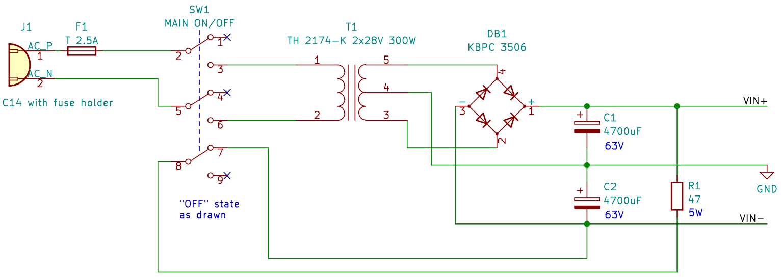
Unregulated symmetrical power supply (click to enlarge)
Note that we are using a 3-pole double throw main switch. Apart from insulating both ends of the primary coil when switching off the device, we use the third switch circuit to connect the shunt R1 across the large storage capacitors. The value and power rating of this resistor is chosen to ensure that DC voltages within the whole device safely disappear within half a second after turning off the instrument.
This also eliminates the possibility of the regulator circuit losing its bearings after switch-off, as the storage capacitors get slowly depleted and the input voltage drops. Without a sizable load, this could easily take several seconds. And a regulated supply that says “goodbye” via raising its stable output voltage to an unspecified level (easily reaching dozens of volts) even briefly, is worse than no supply at all.
The internal stabilized DC is generated by classic three-terminal regulators. We use adjustable ones because we are control freaks and want to fine-tune everything to the last digit of measurement precision on our finished prototype.
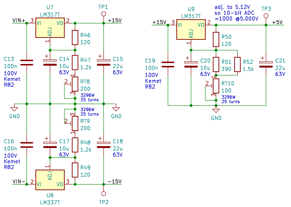
Regulated voltages for internal use (click to enlarge)
Despite all the trimmability, throughout this design we are careful to choose resistor and trimpot values so the midpoint setting on all trimmers is approximately right.
A little trick we use just above is to set the digital systems supply
to precisely 5.12VDC. We will configure our MCU to use its supply
voltage as the analog reference voltage as well. Thus, we establish a
very simple mapping from 10-bit ADC readouts to actual voltages: 1 LSB
equals 5mV. In other words, the readout 1000 corresponds to an ADC
input voltage of 5V.
Control voltages
Now that we have stable internal supply voltages to operate analog op-amp circuitry, we can generate the control voltages according to the front panel controls for output voltage and current limit.
The control voltage AMP_LIMIT is proportional to the desired current limit with a unit conversion of 1 A/V. That is, AMP_LIMIT=1V means the output current is allowed to rise up to 1A before the regulator enters CC (constant current) mode. The same (positive) control voltage is used both by the positive and negative side as well.
The control voltages VREF+ and VREF- are proportional to the desired output voltage. They are, according to their names, positive and negative voltages of the same magnitude. The actual regulated output voltages will be about 3.75x this magnitude, due to the voltage dividers (R7,8 and R22,23) in the regulator feedback loops.
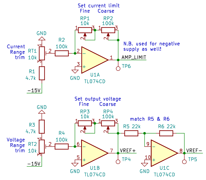
Control voltage sources (click to enlarge)
A trick here is to use the simplest op-amp topology of the inverting DC amplifier, feeding it with a negative reference voltage to arrive at a positive control voltage. The references are trimmable to fine-tune the upper limits of the voltage and current ranges available to the user operating the knobs.
Output voltage regulators
Now we arrive at the heart of the instrument: the actual voltage regulator!
The below image shows one half of it, regulating the positive side. The negative side regulator is essentially a mirror of this, with negated voltages and transistor polarities (PNP instead of NPN). Please refer to the PDF for complete schematics.
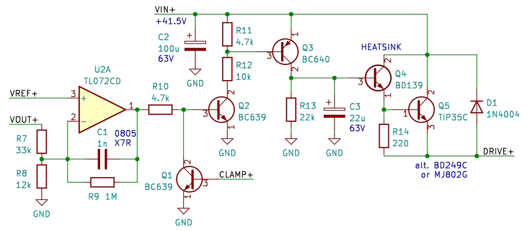
Positive side voltage regulator (click to enlarge)
The op-amp U2A works to minimize the error between VREF+ and a fraction of VOUT+ yielded by the R7,8 divider. DRIVE+ connects to the output terminal through the current measurement sensor. Said sensor circuit drives CLAMP+ positive in case the measured current goes above the limit, and thus shunts Q2’s control voltage. In this case, the op-amp will drive its output towards the positive rail as hard as it can – R10 is there to limit the drive current to a safe level.
The intermediate stages constituted by Q2 and Q3 are needed to bridge the gap between the op-amp output range of perhaps ±13.5V and the voltage necessary to drive the darlington pair Q4 and Q5, which is basically the output voltage minus two diode drops. Due to this many stages and the high end-to-end amplification, the presence of C3 is rather important for stabilizing the control loop and ensuring an AC-free output voltage, even if it means severely limiting the slew rate at which we let the output to swing in response to fluctuations in load impedance. C1, R9 also serve to increase stability.
The pass transistor Q5 is not on the main circuit board, but rather on a separate heatsink (mounted with insulation, as the heatsink is shared with its PNP counterpart Q10) with a temperature-controlled cooling fan. The driver Q4 has a small heatsink of its own right on the PCB.
D1 protects against potentially harmful kick-back spikes from an inductive load.
Output current measurement
The ACS712 is a capable and precise current sensor (based on the Hall effect) in a small package. It looks tiny for the current it is capable of passing through – the 5A variant is perfect for this project, but there is another one for measuring 20A (twenty amps!) in the same 8 pin SOIC.
There is only a small catch: this IC is made to measure bi-directional currents, so its output voltage is half the supply voltage at zero current, and deviates in either direction up towards the supply (for positive currents) or down to zero (for negative currents). We only want the positive half, and the ADC that measures it has an input range of 0 to 5V. So we want some level shifting and gain setting – in short, a linear transformation of the sensor output voltage. (Technically, we could sample the sensor output with the ADC directly and do the mapping in software, but we would throw away half the ADC range.)
The linear transform is performed by op-amps U3A and U3B. The former is used to generate a precise bias voltage of +2.56V (exactly half of the digital supply) on the inverting input of the latter, applying a DC bias to the U3B non-inverting stage. The gain of this stage is set by R17-19, which, multiplied by the sensor trans-impedance of 185 mV/A works out pretty damn close to a nice round 1000 mV/A: 185 * (R17+R18+R19) / R17.
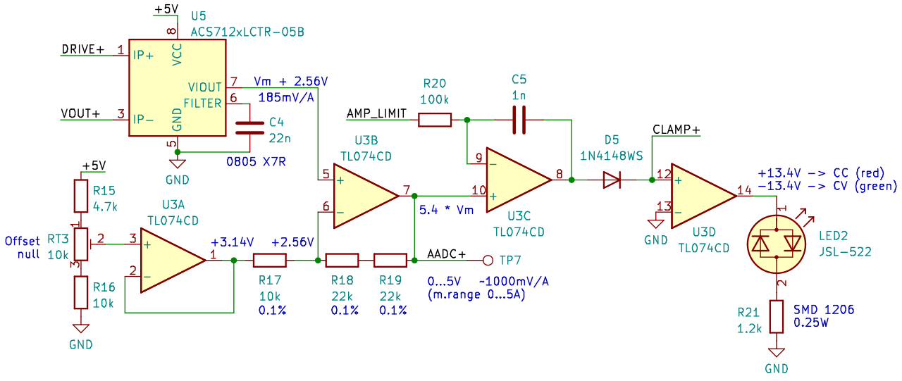
Positive side current measurement (click to enlarge)
So the AADC+ signal will be between 0 and 5V, proportional to output currents between 0 and 5A, with a sensitivity of 1000 mV/A. AADC+ is sampled by an ADC channel for the digital display, but also gets to be compared to the current limit signal AMP_LIMIT by U3C, its output kicking up towards positive supply if the current limit is breached. CLAMP+ opens Q1 in the voltage regulator, as hinted in the previous section.
The fourth op-amp in the TL074 quad package, U3D, is used to drive the dual-color CC/CV indicator LED with either positive or negative voltage with respect to ground, resulting in a normally green light that becomes red to indicate when the current limiter kicks in. D5 is there to relieve its differential input from an unhealthy voltage. (The output voltage of U3C cannot get above two diode drops in the positive direction when current limiting via CLAMP+, but it will swing close to the negative analog rail or about -13.5V when things are normal.)
On the negative side, we do not employ reverse polarities, i.e., the same measurement circuit is used with positive-going signal voltages corresponding to increasing (negative) output currents. We just reverse the ACS712 sensor inputs IP+ and IP-. As a result, we are able to use the same (positive) AMP_LIMIT signal for current limiting and the generated CLAMP- voltage also goes positive when current limiting kicks in. Which is why Q6 is NPN, just as its dual Q1 was, breaking the symmetry between the regulator circuits. (Please refer to the PDF for complete schematics.)
Output voltage measurement
Measuring the output voltage with an ADC is a straightforward matter of using a voltage divider to fit the measurement range to the ADC input range. However, using a 10-bit ADC to measure a signal up to 40V yields an LSB of about 40mV. We would really prefer greater precision than that, especially at lower voltages. On the other hand, we have plenty of ADC channels (eight in total). So a straightforward solution is to use multiple channels with different dividers. The dividers calibrated for lower ranges will overshoot the maximum permissible ADC input voltage on higher output settings, so we must apply some kind of limiting to protect the ADC. In this instrument, I went with the simplest kind of limiter: an 5.1V Zener diode. Is this the best solution? We shall see…
The measurement channel to use will be chosen in software on an ongoing basis, picking the most sensitive non-saturated input. This way, the voltage will be measured with a 10mV LSB up to 10V, a 20mV LSB up to 20V, and 40mV beyond that.
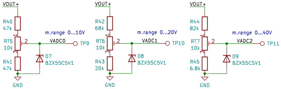
Output voltage measurement (click to enlarge)
Note that we do not measure the negative side output voltage at all. On top of duplicating all the above components, we would also need an additional DC amplifier with negative gain, to make a positive voltage that can be fed to our ADC. Given this cost we decided that this feature was less than essential; our design ensures matching positive and negative voltages (to the limit of component tolerances) unless one or both of the sides enters CC mode. And that is readily shown by the respective indicator light going red.
Digital processing and LED display control
The digital measurement, processing and display is driven by an ATmega328p MCU. Here we use the TQFP-32 packaged variant, and fiercely hope that our hot air chops will be good enough to solder it.
We took great care to design the analog circuitry for best possible ADC performance, which is why L1, C11 and C12 are present as recommended by the device datasheet.
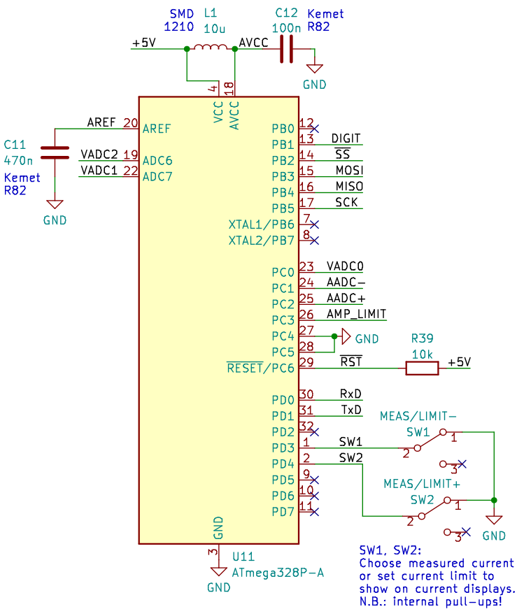
ATmega328p MCU central unit (click to enlarge)
ADC input channels include AADC+, AADC- and AMP_LIMIT for measuring the positive and negative side currents and the set current limit, as well as VADC0, VADC1 and VADC2 which all measure the positive side output voltage as described in the previous section. SW1 and SW2, one for each side, are used to toggle the current display between the measured value and set limit. We spare two pull-up resistors by enabling the MCU’s internal pull-ups in software.
There are ten seven-segment LED display modules to drive in total. We employ two kinds – an orange coloured one for the four-digit voltage display and a smaller, red one for the two three-digit current displays. On the schematic, however, they are part of the same circuit arrangement and are simply numbered U15-U24 from left to right.
To drive them, we employ the ubiquitous time-division multiplexing scheme of round-robin displaying the digits, enabling one digit at a time while setting the common segment lines to its desired values. This is all controlled by the SPI output (SS, SCK, MOSI) feeding 74HC595 registers.
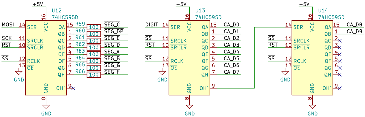
Display control and drive logic (click to enlarge)
In contrast to earlier variations on this theme, here we employ 8-bit SPI transactions that output only the segment data, i.e., which LEDs of the enabled segment should light up. These bits are serially fed into U12 via MOSI. At the same time, enabling the right segment is done with a separate shift register chain made up of U13 and U14, fed by the DIGIT signal and stepped on each SPI transaction by means of using SS as the shift clock. The MCU only has to set DIGIT to “1” on every tenth SPI transaction and keep it “0” at all other times. This “1” will then propagate along the common anode drive signals CA_D0 to CA_D9. Of course, the MCU program must be clever about the sync between the digit enable and the segment code to output, but this feels more complicated than it actually is in the software.
A notable detail is using the MCU’s RST signal to reset the shift registers as well. This does not get any use in production, but when programming the MCU via SPI, it avoids burning in the digit that was active at the moment the programming started. Instead, the registers all get reset and the display turns off.
Note that driving this many LED digits in this fashion is pushing things a little bit. Display brightness is adequate but could be much higher, especially in sunlit conditions. However, we are limited by the current drive capability of the 595’s. The segment driver chip U12 is the tightest bottleneck, as it is always on, while its output current gets spread over 10 displays.
Proportional fan control
The last piece of the puzzle is to control the fan speed of the main heatsink cooling the pass transistors. These transistors will dissipate potentially large amounts of heat, while barely nothing at other settings. Some automatic control would be nice to only drive the fan when it is needed, and only drive it as hard as needed to keep the heatsink temperature from rising too much above a comfortable level.
The solution is a so-called proportional fan control circuit, and this one is basically lifted from The Art of Electronics (Horowitz-Hill, 3rd ed., pp. 608) with some minor adjustments.
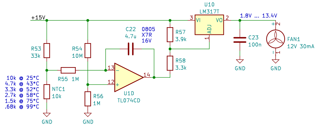
Proportional fan control (click to enlarge)
The LM317 is employed as a power driver, its adjustment voltage driven by an op-amp based integrator. The time constant is set by R55 and C22 to a couple seconds. (4.7 seconds to be exact. However, that would be over-confident language given the tolerance of C22.) The divider R57,58 interfaces the op-amp output voltage range (±13.5V) to positive-only; U10 will drive the fan with the ADJ voltage plus 1.25V.
The NTC, mounted on the heatsink between the two pass transistors, forms one half of a bridge together with R53, the other half being R54,56. The values are set up so the integrator will be in equilibrium at around 50°C. Above this temperature, the output of U1D will slowly start to rise. I was surprised how well this simple analog control works in practice!
Development
As with all substantial projects, development of this instrument was done piecewise, concentrating on one or a few blocks at a time. I first began by sourcing enough loose components to build some partial models on a breadboard, which culminated in both sides of the voltage regulator circuit being separately built one after another (I did not have the real estate to have them co-exist).
After the basic CV operation was deemed stable, I amended it with the current measurement and limit circuit. A lot of time was spent playing with various component values to tune the dynamics of the control loop. Not that I am satisfied – it is still too slow for my taste, but speeding it up I could not avoid some measurable AC (about 10mV) in the output which I wanted to avoid at all cost. Linear regulators are supposed to be quiet, after all.
Then came the fan control circuit, where once again, calibration and tuning of the components proved to be a very time-consuming process. By this time I have sourced the main heatsink (together with fan) from my wardrobe: a spare, intact Pentium III cooler I never got to use. Fortunately, there were some adequately placed holes (originally for the mounting bracket) that I could use for mounting the pass transistors and the heatsink itself. Still, I had to drill a small cavity for the NTC sensor.
![]()
Pass transistors on heat sink, before heating the shrink tubes (click to enlarge)
I detached the temperature sensor of my DCF77 clock and used it as a digital thermometer to see if my calculations had any merit, as I found it hard to judge the heatsink temperature by hand. I got pretty close to 50°C – the below picture was taken with the fan running and heatsink almost in equilibrium.
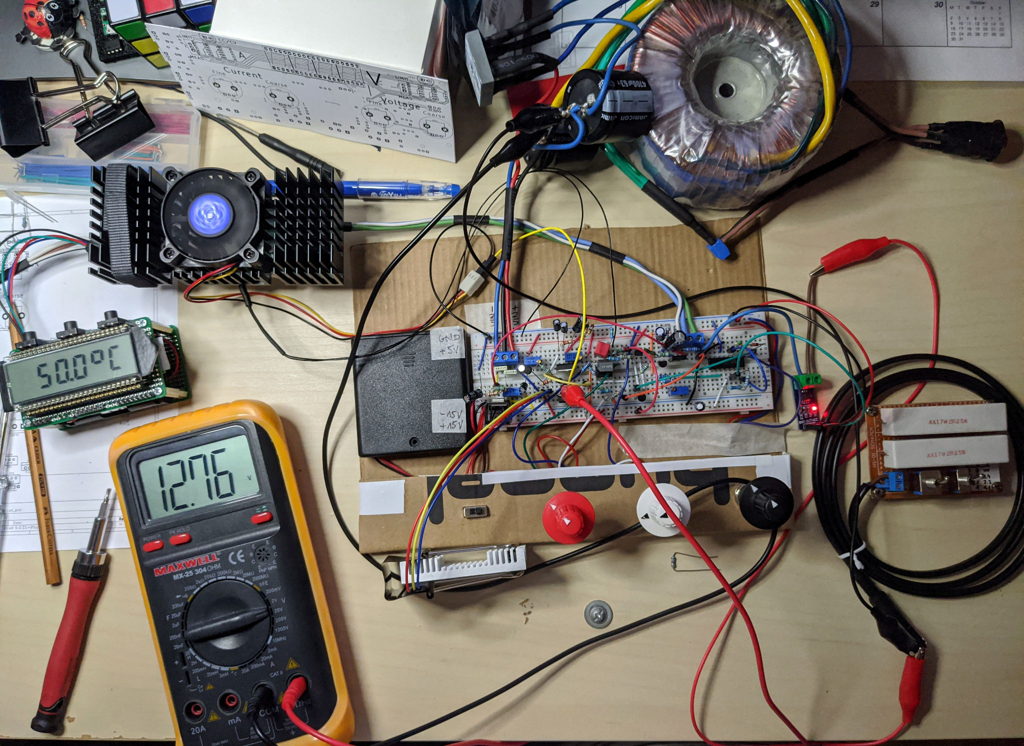
Breadboard version with test load and heatsink temperature probe (click to enlarge)
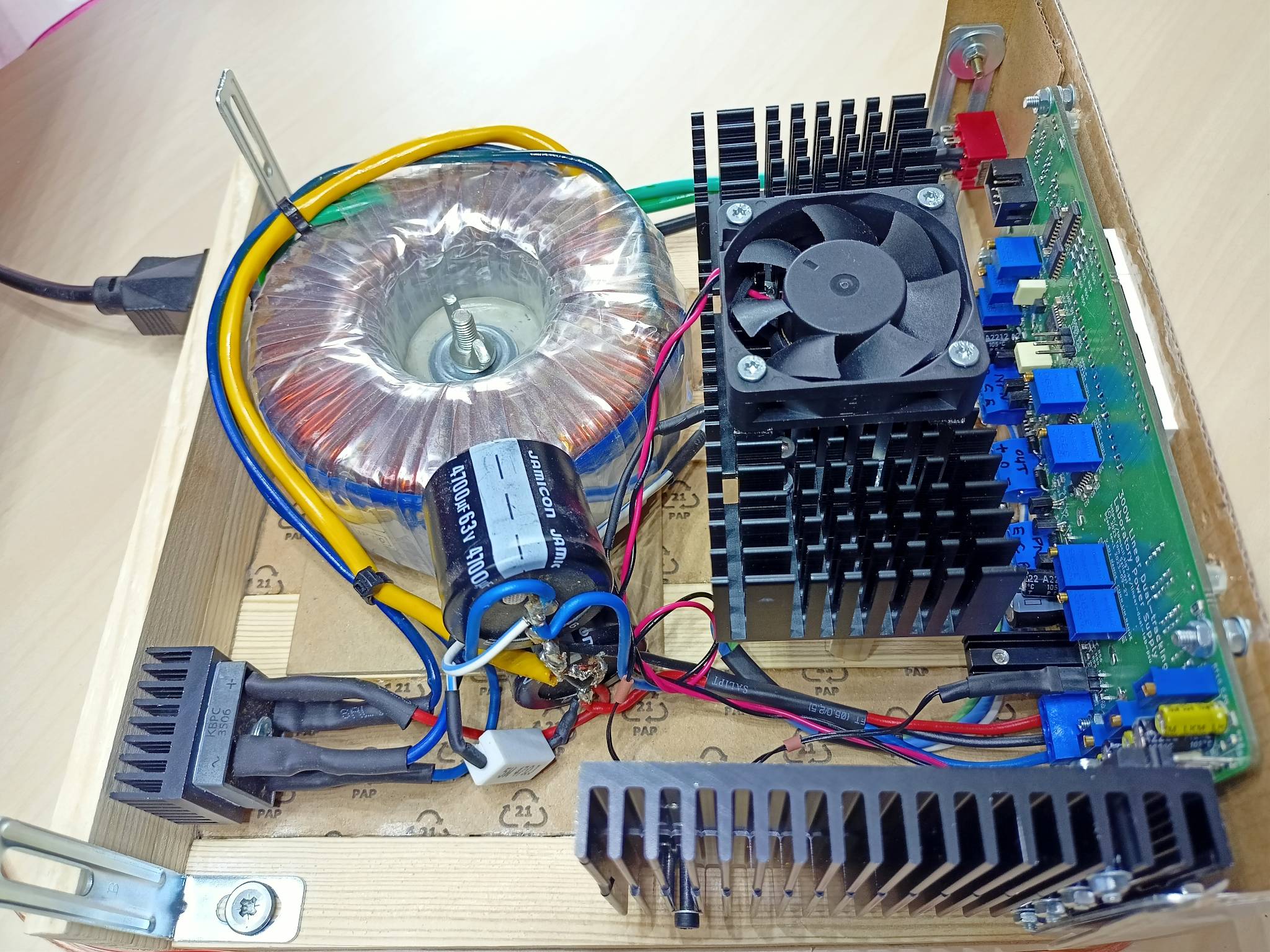
Towards the right of the breadboard, you can see an ACS712 sensor evaluation module (small PCB with red light) acting its part in the current limiter. There is also a resistive test load unit on a larger piece of perf board on the far right. I assembled this out of two large white power resistors of 2.2Ω / 17W each, plus two switches to connect them in parallel, in series, or to use just one of them. The two switches thus allow setting a load resistance of 1.1Ω, 2.2Ω, 4.4Ω or turning it off. The digital multimeter displays the regulated output voltage, subjected to this load.
The silver heatsink to the right of the DMM hosts U7, the LM317 generating +15V. This is the one regulator (of four three-terminal regulator ICs) dissipating the most power. I spent quite some time inspecting all the components by hand, to see if anything needed more cooling than my calculations indicated. I ended up putting small heatsinks on the Darlington drivers Q4 and Q9, and doubling the common heatsink of the four regulators U7-U10. Maybe I am overly conservative, but I would like this instrument to function without becoming an incendiary device. (Do read on to see how well that worked out…)
Simulation via ngspice
A whole new topic I started to dig into while designing the circuits of this instrument was computer aided analog circuit simulation. This is (as I found out) a deep art and science at the same time. I used the open-source, venerable but still actively developed ngspice circuit simulator; I found it has an extremely beginner-hostile manual but at the same time, a nice enough tutorial.
I sourced component models from the appropriate places and started tinkering with models of simple circuits (such as the ones in the tutorial). Slowly I built up a more-or-less complete model of the major parts of my instrument: the control voltages plus output regulators and current sensors for both sides. For the most part, I had no issue finding appropriate models for all the semiconductors. The only exception was the ACS712 current sensor. So I created my first ever from-scratch SPICE model, an extremely bare-bones model consisting of the current-sensing resistor and two linear VCVS (voltage-controlled voltage sources) to set the sensor output: model; test circuit.
The most useful result of this work has been a stepped DC simulation, sweeping the voltage input control from minimum to maximum, with two different loads on the positive and negative sides, hitting the set current limit at different voltages. At each setting, ngspice would compute the operating point – the DC voltages and currents at that particular steady state. I also got ngspice to compute dissipation of several key components. You can take a look at the PDF capturing this simulation as well as the input files to ngspice plus gnuplot to generate that.
As you probably noticed, I am not a fan of fiddling with GUIs – for example, KiCAD ostensibly has some way to integrate with ngspice, to facilitate simulation of the captured schematic. I did not have too much immediate success trying out these functions, and decided that I wanted to peek “under the hood” anyway.
One thing I sadly did not manage to do was to come up with a decent transient simulation of the circuit in response to changes in load impedance or supply voltage. It would have been rather helpful to have this but I ultimately did not have the dedication to do all the research and get it to work. I will probably have to do that for my next circuit though, especially if I really want to design a somewhat more state-of-art, high current switch-mode power supply!
PCB and assembly
At this point I have spent close to a month building subsets of the whole thing on breadboards, tuning component values (on my desk and in my ngspice circuit model), and convincing myself that yes, this might work the way I want it to. I had no way to have the whole circuit assembled in a robust way so I could really beat it up on the bench, unless I went ahead to fabricate it into a more permanent form. And so I did.
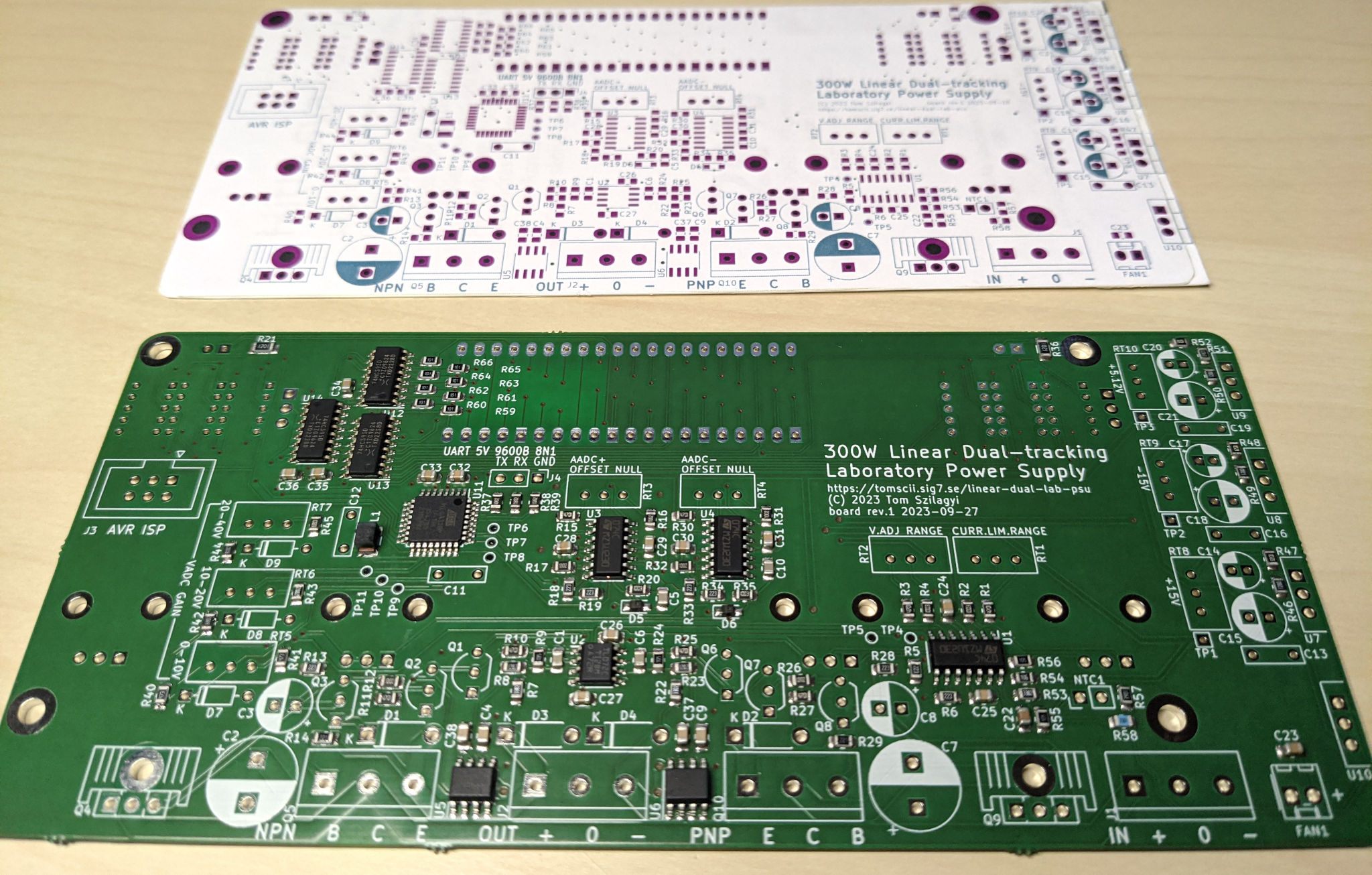
Accordingly, the next two weeks or so were spent in the KiCAD PCB design tool. Central to the design was my desire to place all user-interfacing knobs and displays nicely laid out directly on the PCB (so, no wiring), with the rest of the circuit arranged so it does not take up more space than necessary. I think I succeeded in that regard, using SMT (where practical) and having arrived at a close to optimal component layout. Here are the two layers, front (red) and back (green); note the front is traditionally the side with components. In our case the back has all the (through hole-mounted) knobs and lights facing the operator, but all other components are on the front, facing the inside of the instrument.
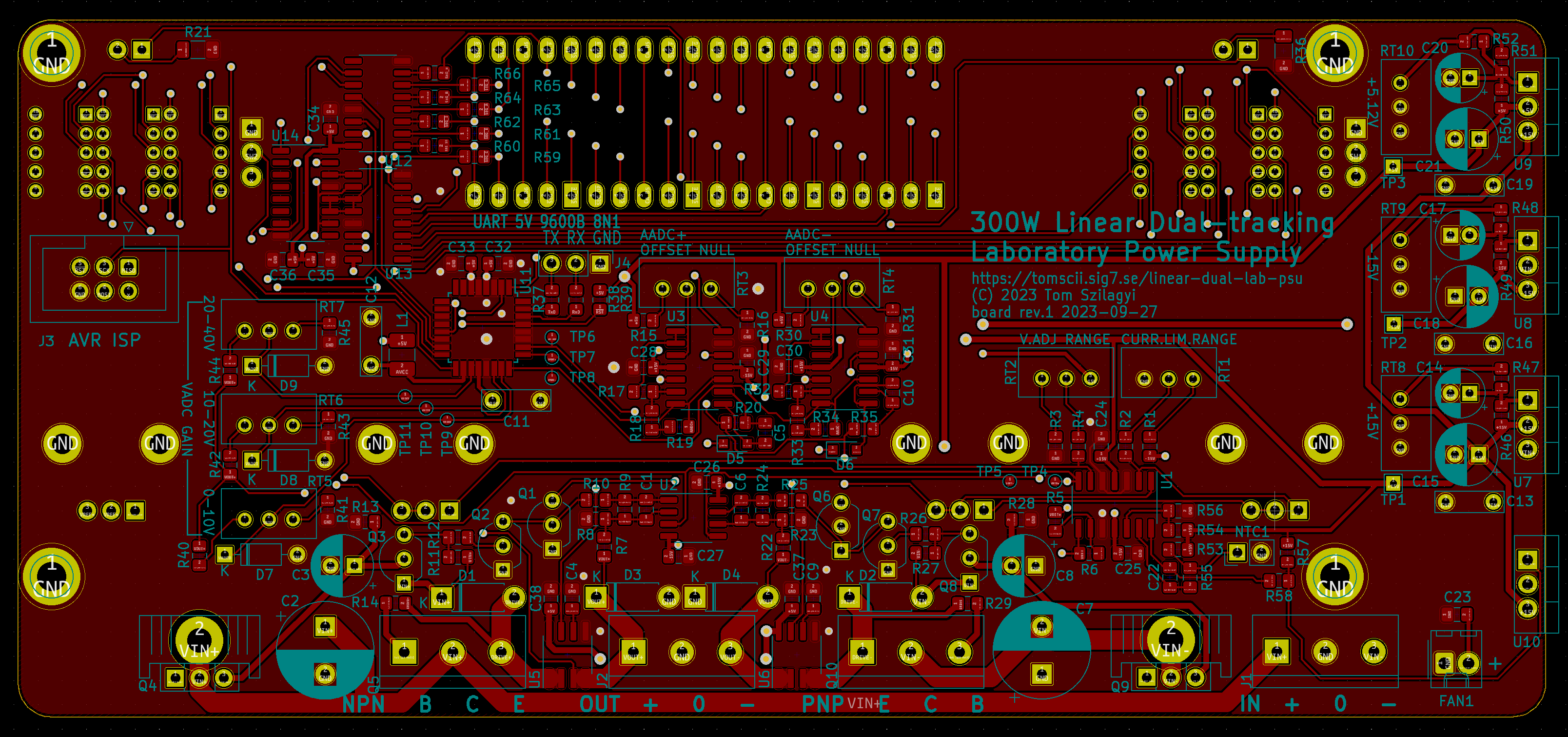
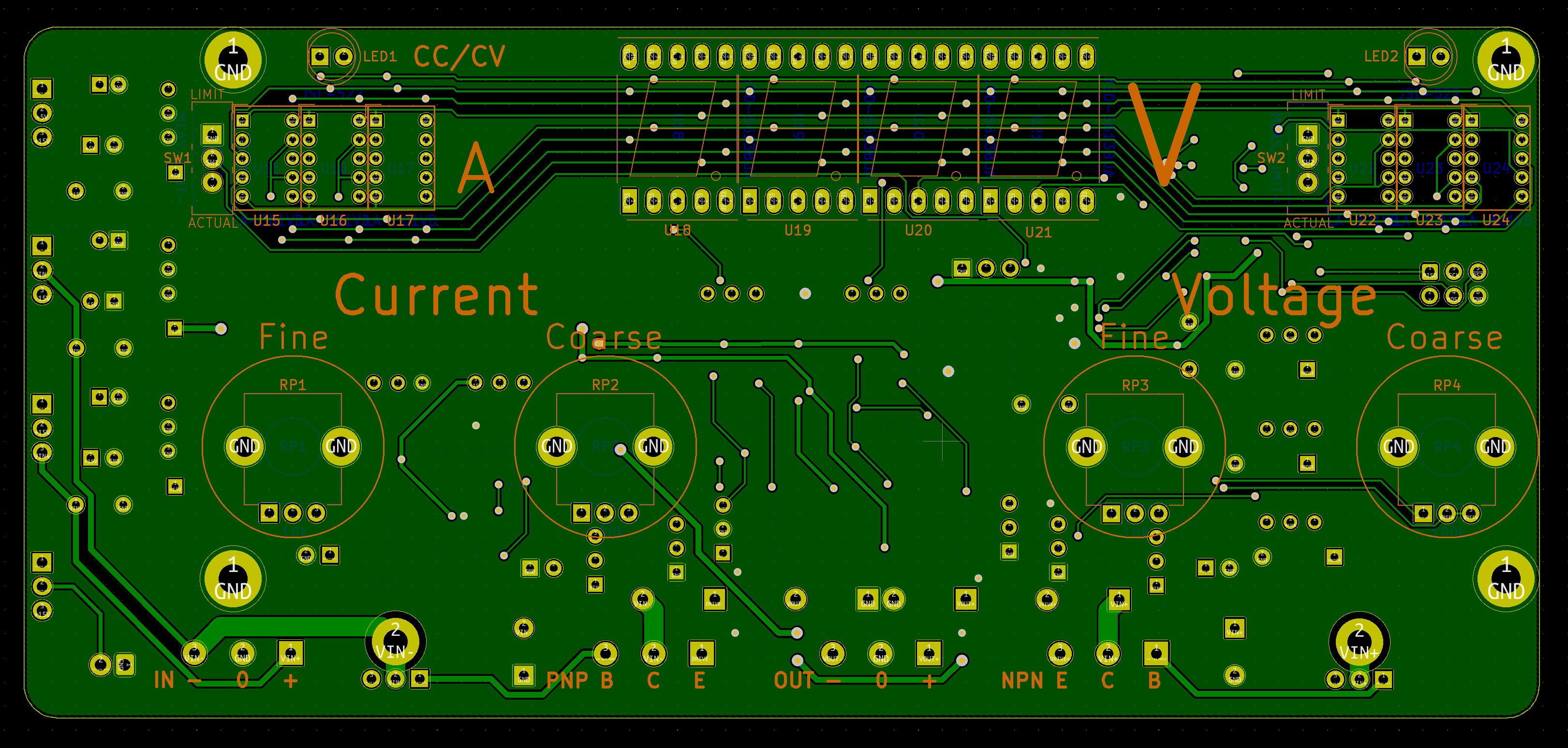
PCB front and back, courtesy of KiCAD 6 (click to enlarge)
I also captured a nice rendering (with ray-tracing!) of the model. Not all 3D component models are fully appropriate, but overall, it comes close enough to be useful. Q4 and Q9 heatsinks are missing though, and the leads of the small red LED-display modules, protruding from the other side, are a little off.
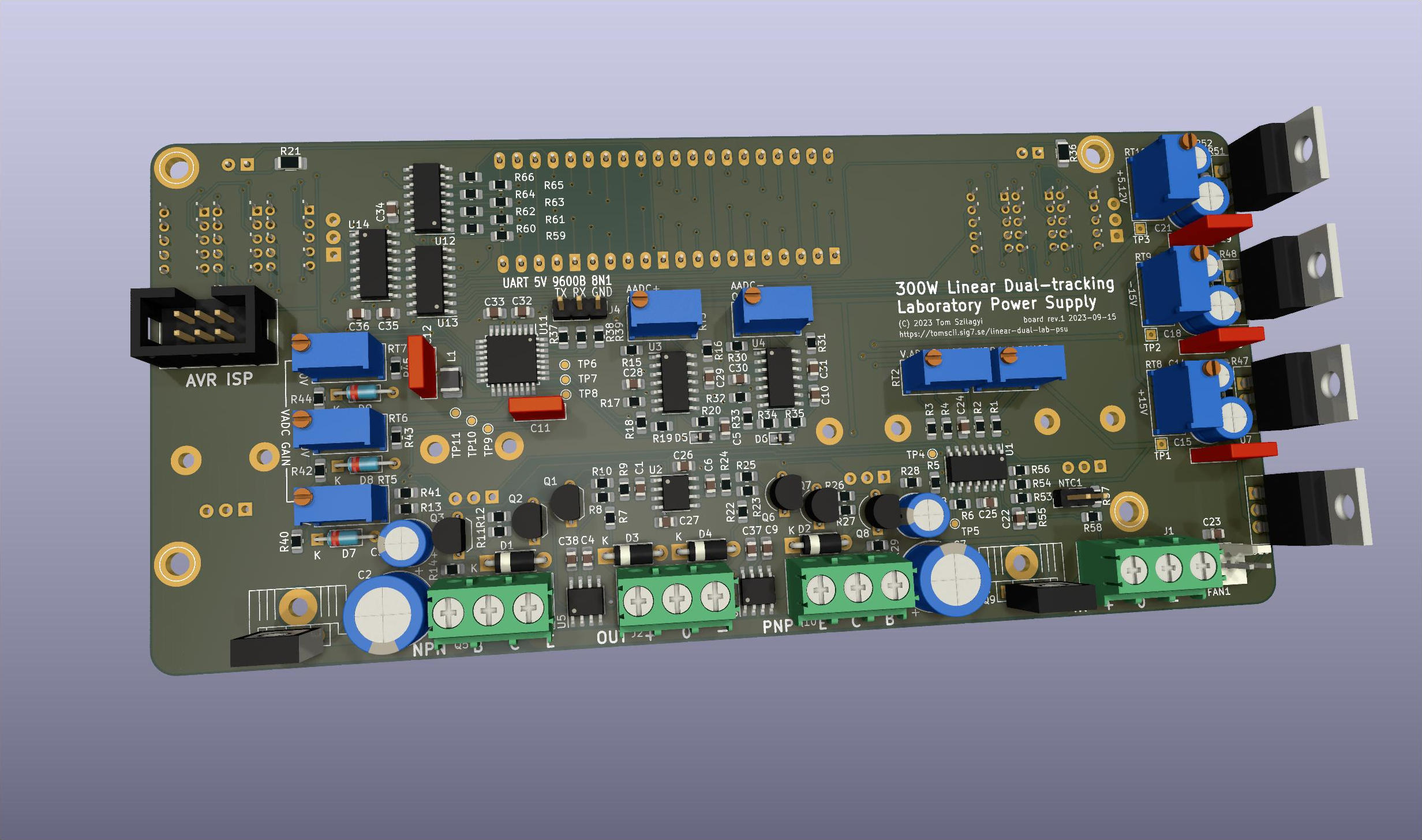
3D model of PCB, courtesy of KiCAD 6 (click to enlarge)
Another habit I have gotten into is to print out 1:1-scaled PCB layouts on a regular office printer, glue both sides on some thinner cardboard and make a paper model of the PCB. This is a rather cheap way of really making sure that critically spaced components do in fact line up. I was especially keen on doing this as I had to create the PCB footprints of some of these components myself.
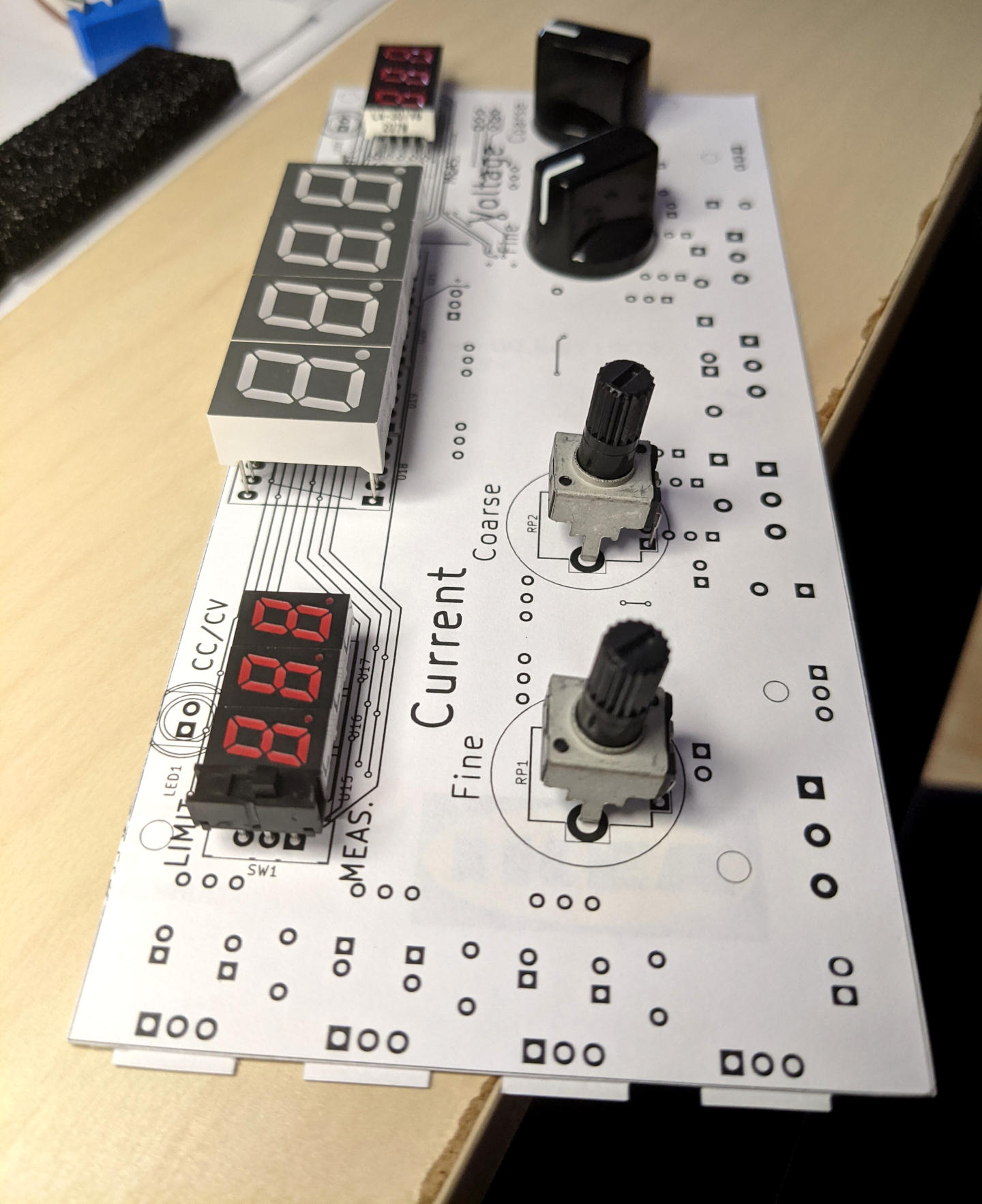
Cheap insurance against egregious design errors (click to enlarge)
Once I had gained a high level of confidence in my PCB design and caught myself rattling over inconsequent small details (a sign of the design having appropriately converged) it was time to finally place a manufacturing order. When the boards arrived a couple weeks later (and I was happy that unlike last time, they did so with all connectivity tests passed at the factory!) I got into action with my hot air solder station.
The below image captures the board just after I finished all SMT soldering. In retrospect, I should not have worried about the TQFP-32 packaged AVR MCU at all. Soldering it went like a charm, and I was really pleased with the result.
Board after SMT assembly (click to enlarge)
The rest of the components were summarily soldered with my regular iron; no surprises or hiccups.
Next came the issue of housing. I did not find a suitably sized factory-made instrument case to buy, so I made a custom bottom structure out of light wooden spacers with cell-structured cardboard fillers in between. This strong but light bottom plate was used as a base to fasten some metal hinges in all four corners (out of my pile of leftover IKEA stuff) to hold the front and back plates. Considering the mechanical stress the banana sockets will be subject to, I cut a further piece of wood spacer to size, drilled holes for the banana sockets and screwed it across the bottom plate.
The rest of the front plate was made of thin cardboard (yeah, I know – alas, I don’t have access to a machine shop to work more durable plastic or metal plates with high precision). The print was drawn in KiCAD as yet another layer in the PCB design; this made it trivial to perfectly match the component spacings. I printed it out, glued it to the cardboard already cut to size and stuck a self-adhesive transparent laminating sheet on top. I folded in the laminating sheet by the edges. Then I proceeded to make cutouts for the LED displays and control pots with a sharp knife.
Profile view (click to enlarge)
At this point I basically got bored and decided that I did not mind the rest of the case missing. It’s going to get warm anyway, so having excellent ventilation is not a bad thing. Some day I might find some sheet material to bend along two parallel lines, to make a cover plate for the top and the sides.

Side view; helicopter view (click to enlarge)
Calibration - we’ll fix it in the software!
So now I had a working, complete, finished (according to my definitions) piece of kit. Well, except for those pesky little trimmers I sprinkled rather liberally all over the schematic, for fine-tuning everything to the last digit of my measurement precision.
Now is the time to do it! I started with the fixed internal power supplies, did the +15.00V, -15.00V and +5.12V dance in that order. Only to realize there is this thing called tempco (temperature coefficient) which means that the operating point will slowly drift away as the components warm up. Ouch! Not much to do about it now (I really need to start digging into chapter 5 of The Art of Electronics, which is about achieving precision in electronic circuits). In the absence of any clever idea, I arbitrarily set my calibration target as the thermal state 20 minutes after a cold turn-on. That turned out to be usable.
Okay, on to the voltage and current measurement circuitry. In the latter circuit, I had (wisely) relied on the datasheet specification of the precision ACS712 having 185mV/A of trans-resistance, so I did not include any gain calibration, only null offset calibration. That gave me some headaches (that evil tempco again: apparently everything you think about as a constant is in fact going through some slow motion) but eventually I settled on an acceptable setting and decided to leave those trimpots alone. Notes to self: 1. I really need to ditch the TL074 (with its substantial offset voltage and drift) and migrate towards some more modern, higher precision op-amp – at least in measurement circuits! 2. Ngspice also supports simulating temperature drift (it is possible to specify the temperature at which the components are simulated, so tempco effects can be, and are, taken into account)!
That left me with the voltage measurement calibration, the one I was most confident about (hey, it’s a plain old voltage divider!) and did not expect any issues at all. I expected it to be pretty accurate out of the box. Except… the readouts were all over the place! I could discern some kind of saturation effect, where the supposedly linear below-breakpoint transfer characteristic of my limiter (remember, to protect the analog inputs of my MCU from overvoltage) would become a rather leisurely upwards-flattening curve. Only to be punctuated by the automatic switches to the non-saturated channel with the largest signal. Producing weird, weird numbers!
I ultimately chalked this up to the zener diode in my divider having a “soft knee” and starting to conduct to a small degree, but enough to utterly destroy the voltage divider’s precision! A better solution (as I have learned after perusing this AoE brick of mine, an excellent all-round brick!) would have been to put a regular (non-zener) diode between the ADC input and the 5V in reverse, conducting when the ADC input is above supply plus a diode drop. Or maybe no diode at all, as that input is bound to have a similar protection diode built in. Well, better do it right next time!
What did I do this time? Of course, I did what any reasonable software person would do. I measured the characteristics of my grossly non-ideal divider with my rather precise digital voltmeter, and put a couple calibration tables in the software converting ADC readouts to digital voltages, with linear interpolation in between data points. There, I fixed it! The voltage display started behaving sensibly, and with some further fine-tuning, in the end I got pretty accurate results!
I could probably remove the Zeners and the calibration tables and rely on the internal protection diodes of the ADC inputs but hey, I now have an accurately working solution!
Conclusion
And with that, the instrument had come into existence and was summarily enlisted for daily production. It seemed to work precisely as intended. I stress-tested it with loads of several amps (even the rectifier bridge would get hot, which is why I retro-actively installed a passive sink for it, visible above). Most of the time, though, it served as the power supply to my LED Superlamp, spending countless hours in the winter darkness feeding 700mA at 38V or so to a series string of twelve bright light LEDs.
Here it is, proudly stretching across my (tiny) desk:
Bench supply in its natural habitat (click to enlarge)
As usual in all my electronics projects, I gained a great deal of practical new knowledge and experience. Also, not everything went as planned – analysing the faults seemingly inevitable in an initial prototype provide the most valuable lessons! I would definitely not build this again in unchanged form, but it has already become an indispensable piece of kit.
As usual, all the sources for this article (including the KiCAD hardware design, the project for the on-board firmware, plus ngspice simulation files) are published online with everything licensed under the terms of the very permissive MIT license.
Update: I have a follow-up, in which the device burns out, then gets cracking. Check it out!