SMT and the ultimate LCD-SPI interface
After having completed several electronics projects from idea to finished gadget, and gained experience with self-designed PCBs, I felt it was finally time to face the elephant in the room. What elephant? The predominant electronics technology I never dared to touch before: SMT a.k.a surface-mount technology. Given that virtually all industrially produced electronics is surface mounted, and has been for several decades, there is a ceiling of how serious you can get before coming to terms with it. And that ceiling is pretty low.
As a hobbyist, there are obvious advantages and disadvantages to SMT, which, in one way or another, all come down to the greatly diminished physical size of the components. Reduced footprints lead to denser, and thus smaller and cheaper-to-order PCBs. That is pretty good in itself. Also, reduced physical dimensions virtually guarantee better electrical properties (less stray capacitance and inductance) – if you have a project where it matters. On the downside: those reduced footprints mean you basically lose your ability to work without a strong magnifying glass and desk lamp (the two ideally rolled into one), plus a tweezer in your (shaky) hand. All your fingers are now thumbs, get used to it.
The most obvious downside, however, is that you can no longer stuff components into a breadboard and experiment to your heart’s content. What was a nice (final) touch of quality and dedication is now a mandatory step: you really need to design a custom PCB and have it manufactured. Oh, and you need to be able to solder the parts. To me, this last step was the most intriguing of all. How do you solder under a microscope? Sure you can amplify your vision with the help of some optics, but your hand is still shaky and your soldering iron’s tip looks enormous under that looking glass, compared to the minuscule leads on all those ICs… and there are tons of them! The few SMD components I could not avoid on my earlier design (the micro-USB socket and LiPo charge controller chip on the EMMA SuperTorch) were tricky enough to solder with a regular iron.
Such was my initial state of mind when I set out to clear this up and decided to do some research. I had some faint idea of how industry does it on a large scale (robots everywhere!), but I have never been to the practical side of smaller-scale operations: where mortals do it with their hands. So it was with some surprise that I discovered that people do not, in fact, use a soldering iron at all. At least not to solder in (and out!) those many-legged spider bugs. They use something else: a hot air gun, frequently referred to as a Hot Air Rework Station.
So I bought one! (For the curious: it is an Atten ST-862D. Good specs and very reasonable price. I bought a set of angled nozzles as well, which do not come packaged with the unit. After testing them out, I believe the angled nozzles are essential for electronics work.)
I blew some hot air on some electronics garbage lying around, and I got pretty good at pulling off some of those insects from the boards. Connectors, even! To someone who has only ever used a simple soldering gun, getting those many-legged packages come off in one piece really felt like magic. And not hard at all, given the hot air temperature goes all the way up to 480°C (and I was not afraid to let it loose on the scrapped boards)! Never mind the thermal shock – I have no plans to use those parts.
So now I had the essential tool to tackle surface-mount technology. And quite naturally, I now wanted to build something with it. And in light of what all this new (to me) tech represents, I decided to industrialize my operations: I would build an electronics module. Something that could be used in several different applications (appliances). And I would manufacture several identical copies of my design. I’m really not used to doing that! It’s almost like having my own factory.
A new LCD interface
One thing that had bugged me all along was how complicated and messy my ad-hoc LCD driving circuit became on the DCF77 clock I built. The hardware got bulky with a lot of logic (several eight-bit shift registers, taking up most of the board surface!), and the software had a lot of bespoke bit-banging code. But if these issues could be sorted out via using board space-economic SMT and MCU cycle-economic SPI, that lovely six-digit LCD would be an attractive choice in so many places: various clocks and timers, meters, etc. I have a couple ideas already, but this whole display better be a module with a simple-to-drive interface!
In my WiFi-clock I implemented a time-multiplexed LED display driven simply and economically via SPI. The same operational principles of SPI-to-parallel conversion (stuffing data into a set of registers) apply to driving an LCD. With an additional wrinkle: one has to keep altering the polarity of the signal. I.e., the COM (common) node of the LCD has to be a dynamically driven signal as well (as opposed to being statically tied to ground). It must be driven with a square wave of alternating zeros and ones. And all the segment-driving signals must be set with respect to the momentary state of this COM signal. A transparent (OFF) segment is produced when the segment signal is identical to COM; the segment is dark (ON) when it is driven by the COM’s logical inverse.
It would be really beneficial if this alternating phase could be built into the LCD driving hardware, together with the serial-to-parallel registers. On each SPI write (serially shifting in the bits) the polarity would be automatically reversed. The host performing the SPI writes would not have to care about any of this, only write the bits representing the logical state of all segments (0: OFF, 1: ON) as is on each write.
So after a bit of thinking, I came up with this piece of logic:
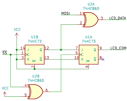
LCD phase-alternating logic
All it takes is two JK flip-flops and two 2-input XOR gates. Here is how it works:
-
The start of the SPI transaction is signalled by a falling edge of the low-active SS signal. This slave select signal stays low under the duration of the subsequent write. The ‘73 is a JK flip-flop triggered on the falling edge of its clock. Thus, U1B is conveniently triggered each time an SPI write is just about to start.
-
As U1B’s J and K inputs are both wired to VCC (that is, logical 1), its output will be negated on each trigger. So, to introduce some terminology: every second SPI write will be an inverse cycle (when Q=1), the others constituting straight cycles.
-
It is immediately apparent that U1B’s Q is used to control an inverter on the MOSI input. If Q is logical 1, MOSI is inverted by U2A. Else, it is let through. (When thinking about this kind of logic, I frequently find it helpful to think of an XOR gate as an inverter with enable: any of the inputs can be seen as a toggle for transferring the other input with or without inverting it). So LCD_DATA (that feeds the registers) will be equal to MOSI (the data from SPI) during a straight cycle, and its negation during an inverse cycle.
-
Now we only need to understand how LCD_COM works. It is output by the JK flip-flop U1A triggered by an inverted SS (U2B is permanently wired to act as an inverter). So U1A will trigger on the rising edge of SS, that is, at the end of the SPI write. This same edge is what makes the ‘595s latch their outputs to the shifted-in content! I.e., this is the moment when all the LCD signals change.
-
And at this moment, U1A will sample its J and K inputs, which will always be logical inverses of each other. In such a configuration, a JK flip-flop acts as a D flip-flop (with D=J). Thus, when U1A samples {J=1, K=0} at the end of an inverse cycle, its Q (and thus LCD_COM) will become 1, and on {J=0, K=1} at the end of a straight cycle, it will be 0.
And this is exactly how we wanted things to be! The LCD_DATA feeds a chain of ‘595 shift registers (as usual) and those are stepped by two clocks: the shift register clock (shifting individual bits along the chain) is driven by the SPI clock, and the output latch is clocked by the rising edge of SS. Just like in the WiFi-clock.
All the SPI host has to do is write the same data representing segment states, in straight encoding, periodically into the device. Preferably at a refresh rate of 100 Hz or more (for the sake of the LCD). But this is trivially handled by SPI interrupt handlers, so should be pretty much transparent to the host program and present minimal load to any MCU.
The complete schematic is shown below. Click on it for the fully sized sheet or download it in PDF via the link:
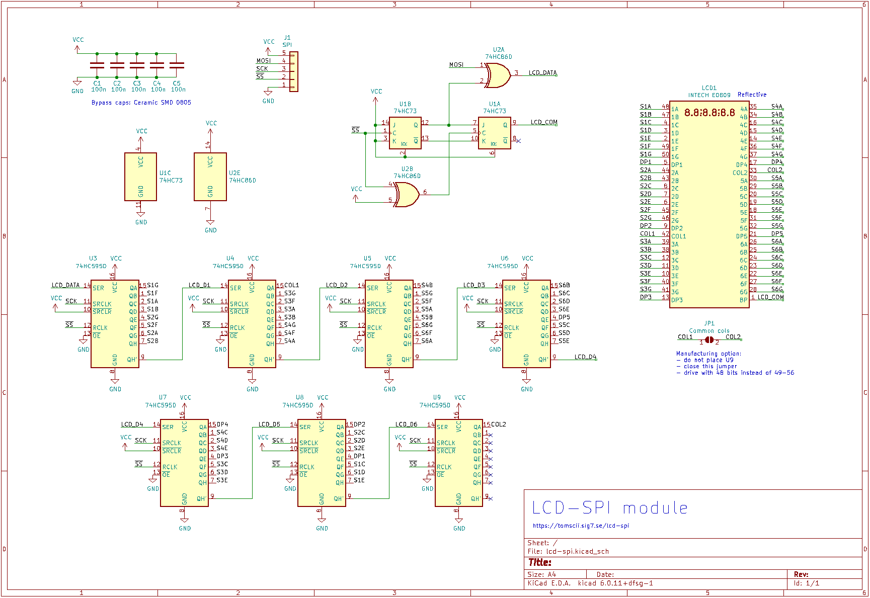
Schematic (click for full resolution), PDF
One noteworthy detail: There are exactly 49 segments on the LCD, which is one bit over that which fits in six eigth-bit registers. That’s kind of a bummer; a whole package (a seventh register) for only a single bit? Feels like a lot of waste. Can we get rid of it somehow?
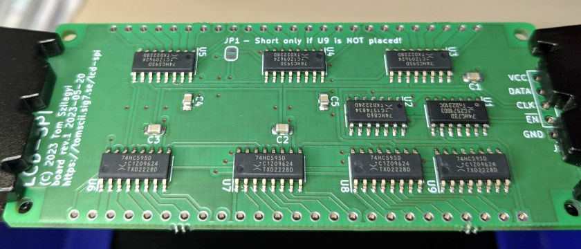
We could, if we decided that we do not ever want to separately control the two colons. I made this choice in the DCF77 clock but here we have a different situation: this is a module for embedding into an as of yet unknown device, so we would rather not restrict what the hardware can do. So as the circuit designer, I left a choice for the manufacturer (my future self): either they can populate the seventh register and have full control over all segments, or leave U9 unpopulated but short the solder jumper JP1. This way the display will be controlled by 48 bits only, at the cost of the two columns wired together.
PCB design
Board dimensions were dictated by the size of the LCD display, with some space on the sides large enough to fit the connector onto one of them. The LCD lies smoothly on the surface of the “back” side (where there are no components - and no soldering either). SMD components are placed on the “front” side. Tracks are 8 mils (0.2 mm) wide and vias are 0.8 mm in diameter (0.4 mm holes). These are vanilla specs for any PCB manufacturer.
A fairly obvious consequence of going SMT is that everything wants to be on the same side of the board: the component side and the solder side naturally become one and the same. You explicitly need to force wiring onto the other side (if you need to) by placing vias.
I definitely saw the need and ended up with 49 vias in total, in no small part due to my desire to thoroughy connect all unused areas (on both sides) into a supply plane sandwich: the side with the LCD on it is VCC and the side with SMD components is GND. This strategy resulted in the need for many vias near the packages’ supply pins.
The interface labeling deviates a bit from SPI notation: the active-low peripheral select (normally SS) is called EN and the incoming data (normally MOSI) is simply DATA.
Here is a 3D render of the end result (with the obligatory rounded corners):

3D model of PCB rev.2, courtesy of KiCAD 6 (click to enlarge)
Did you notice that I presented you with revision 2 of the PCB design? If yes, well spotted, and stay tuned for the juicy details… but now time for the fun part!
Assembly
Soldering SMD is done with a hot air gun (unless you happen to own or build your own reflow oven, which I consider just a little bit out of scope at this very moment). But what about the solder itself? That also needs to be SMT-specific.
Indeed: instead of plain old solder, something called solder paste is used. This is a mixture of microscopic solder particles in flux, which, when heated up to the right temperature, becomes solder and starts wetting the contact surfaces around it. While fresh, it resembles dark gray sand that is a little wet.
Solder paste in small hobbyist quantities usually comes in a syringe and if one is extremely good at it, I suppose one can apply the paste with no further ado to some pads on the PCB. With just a couple SMT components and few leads, this might even work (I haven’t tried)!
But the average circuit is too complicated for that. So what you do is when ordering the PCBs, you also order the stencil mask, a thin plate of steel precisely cut to have holes over all the places where you want to deposit solder paste. When you are ready for assembling your board, you place the stencil mask over the board and carefully align it and somehow fasten it in place. Then you squeeze out some solder paste on top of the mask and try to force all of it into the holes with something called a squeegee. Yes, you can buy such a thing expressly made for SMT, but I just used a credit card-sized piece of plastic with great success.
On the other hand, you do have to buy solder paste. Not yet fully confident in my hot air skills, I chose a ChipQuik variant with the lowest melting point I could find: 138°C (that’s right) in the hope of getting away with a lower setting on the air gun and thereby reducing the risk of undue thermal stress to the fresh components.
I picked a piece of cardboard about the same thickness as the PCBs, and cut a hole in it to tightly match one board. I laid the stencil mask on it and aligned the holes carefully, fastening the mask on one side with tape so it could be folded up. I checked that everything looked and felt right and proceeded to apply the paste. It was a bit awkward at first but I quickly got the hang of it. Eventually, after carefully lifting the mask, I saw nice little islands of gray-ish paste deposited on the contact areas. They seemed to be spot on.
Needless to say, I made sure everything was spotless, free of dust and finger smear. It’s a far cry from a clean room, but I tried my best! Here you can see my setup with solder paste, non-official squeegee, and extremely ad-hoc (but very well working) stencil frame, just after use:
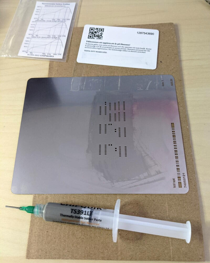
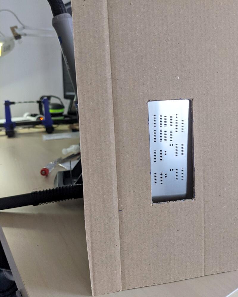
Solder paste dispenser; stencil mask with ad-hoc frame (click to enlarge)
Now came the most critical part. Working under the magnifying lamp, I proceeded to place the parts, very slowly and carefully, in the correct places, with my best tweezer. As I found out, it’s best to let go of a component directly above its intended place without actually sticking it into the paste. It will sit on top of the paste layer (too light to sink into it) and will stay there even if later adjusted with extremely careful lateral nudges.
Below you can see how it looked after components were placed. Notice how the 0805 capacitor sits on top of the paste layer as thick (or rather, as thin) as the stencil mask: 100 μm or 0.1 mm. In other words, a strand of hair.

The dough is ready to bake (click to enlarge)
Time to turn up the heat! I set the hot air station to a conservative 170°C and cautiously low airflow power of 5%. I knew from my initial experiments with trashed boards that a stronger airflow might easily blow away (or at least nudge out of place) smaller parts while the solder is still loose.
I applied hot air with circling moves starting at a distance of about 30 cm, slowly heating up the whole board, gradually moving closer and closer to raise the temperature locally. All the while keeping a close eye on the board through the magnifier lamp. I started to focus the heating to one of the corners. After a couple minutes the solder paste underwent a phase change: in a few seconds, its color went from matte gray to shiny metal. It finally looked like molten solder. At the same time, some of the components moved slightly, all by themselves. At first I was alarmed, thinking that I blew them too hard, but it turned out all good: the parts were moving in the right direction, actually assuming their correct places! This is just the surface tension of molten solder in action, but it feels magical!
I went through the whole board and kept circling above each area until all solder paste was converted to shiny metal. It must have taken somewhere around 10 minutes in total (I must admit that I totally lost track of the time). Below is the end result:

Freshly baked buns! (click to enlarge)
Looks delicious if you ask me. Time for some tests!
Software
This board does not have any software of its own, but I wanted to try it out anyway. So I whipped up a bare-bones project with an Arduino Nano (with my old friend, the ATmega328p on it) on a breadboard to drive it, and perform some quality assurance on the manufactured goods!
Operation is straightforward and minimal:
-
The main program initiates a refresh of the display via SPI writes at a refresh rate of 100 Hz, and updates the display (including decimal dots and colons) once per second driven by a counter and some modulo calculations. This is the topmost layer in the software stack.
-
The SPI module handles multi-byte transmissions under interrupt control. This is the lowest level, driving the actual hardware.
-
In between the two, the LCD module renders operations on digits, symbols, dots and colons into bit manipulations on the data to be sent by SPI.
I feel that all this is fairly straightforward as expressed in the C
programming language. I hope you will agree if you are so inclined as
to check out the code. There is a small piece of conditional
compilation: uncommenting the define of JP1_SHORTED in lcd.h will
make the software adapt to a board populated in the alternate manner
(with one less register and 48 bits of state enabled by common
colons).
The SPI and LCD modules are intended to be copied into any application project using this display module, and this project acts as a fully functioning demo for them. The handling of SPI is of course AVR-specific, so it would have to be rewritten for a different processor, but not by much – all architectures should have equivalent interrupt-based facilities!
Here it is all in action:
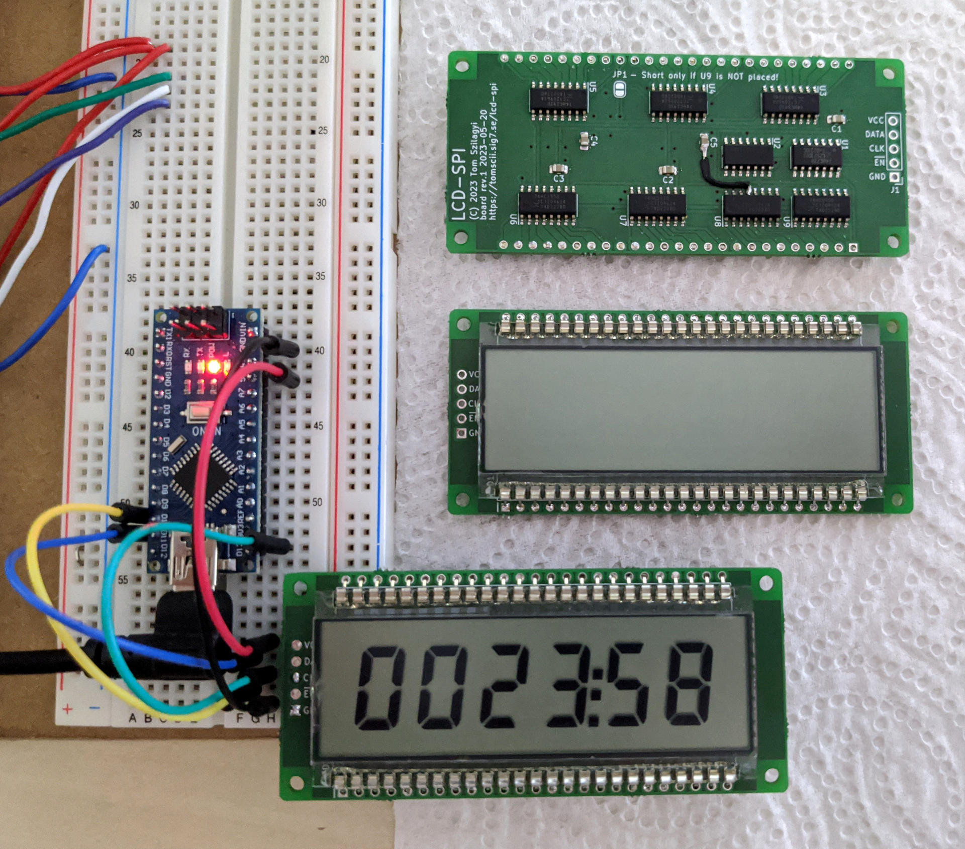
Hardware + software: demo with an Arduino Nano (click to enlarge)
Hitting a snag!
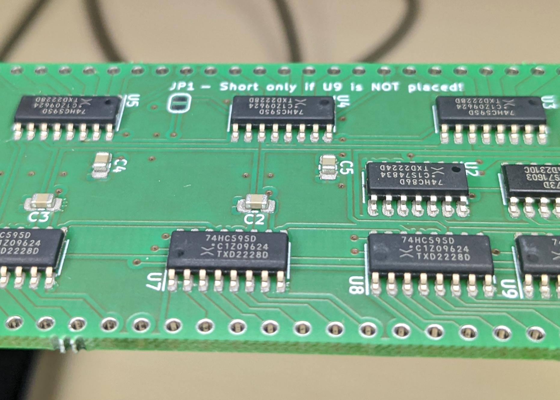
So now we reached the end and you are thinking, what about that rev.2 PCB? And what is that black patch wire on the upper right above? Yeah, I was just about to tell you.
In all the photos of actual PCBs, you saw the original (rev.1) design, because that is all I got fabricated so far. Unfortunately, when my batch was done, AISLER kindly informed me that my board’s automatic connectivity tests have failed. Bewildered, I checked out their report and saw the exact same issue reported for all six boards. There was a single unconnected net! Based on its name, it was easy to identify in KiCAD. And then I looked at the pre-fab board view again and it finally clicked:
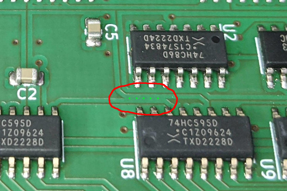
A gap in the ground plane fill! (click to enlarge)
A thin track of copper ground plane fill should have remained in line with the green marker dots. It got removed by AISLER while processing my uploaded KiCAD project.
I double-checked that the track satisfied the minimum width requirements in KiCAD. I remember I was careful to run a DRC (design rule check) beforehand, and sure enough, it still looked good. Close to the limit, but good. Clearances also appeared sufficient. However, AISLER must have somehow treated the filled copper area differently than regular tracks and I suspect there must have been some copper reduction going on, making the track disappear as its width was no longer above the supported minimum.
The only consolation I found was that AISLER’ pre-fabrication board view did correctly show the absence of this copper. I should have noticed that, but I did not. So the fault lies with me, and the moral is, always thoroughly check the manufacturer’s pre-fab view, because you might be surprised. At least now I know to be extra vigilant around filled areas!
Correcting this in the design was trivial; I made sure to draw an actual 8 mil track in there and not rely on the ground fill for the connectivity. Sure enough, the pre-fab view looked correct on this new revision. I also fiddled a bit with the fill settings and slightly decreased the clearances (in anticipation of some further thinning).
Oh, and the manufactured boards… they all have those ugly black patch wires on them. Once I run out of LCD modules, I will make a new batch with the correct PCB.
Conclusion
Having finally conquered surface-mount technology feels like having gained a superpower! Now I can tackle much more complex and demanding hardware projects, use almost any type of modern component in my designs (except BGA and similar packages, which are still out of my league) and in general, be a little closer to the state of the art in electronics!
The circuit itself presented here was fairly small and trivial, if useful as a demonstration of principles. But fabricating it has provided me with a whole gamut of valuable learning experience!
As usual, all the sources for this article (including the KiCAD hardware design and the demo software described above) are published online with everything licensed under the terms of the very permissive MIT license.