DCF77 clock with temperature & humidity sensor
With our backs just turned on the latest DST adjustment ritual (how many clocks do you have to manually set in your house twice per year?) I got reminded of my single clock that does not need adjustment. And not only around daylight saving shifts. In fact, this is the clock I use as a reference when setting all other clocks. Needless to say, it’s my favourite.
This is the story of the DCF77-based clock I built some time ago, and works so well its presence on my small desk is now taken for granted.
Beginnings
It all started with a bog-standard, cheap DCF77 receiver module from Conrad floating around my drawers and my desk. I don’t recall when I bought it, but it must have been many years ago… and I have never gotten around to using it. So I decided to change that.
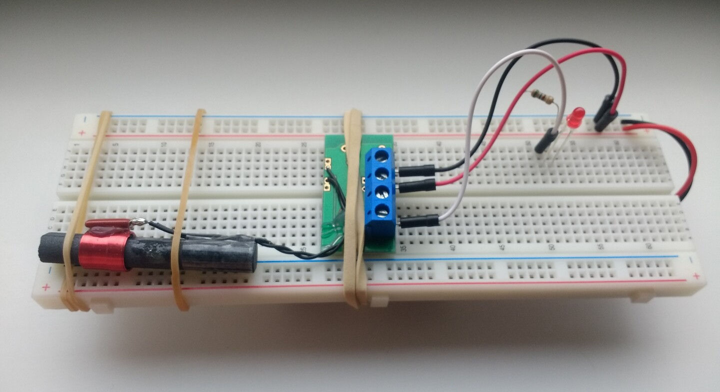
Receiver test kit, battery pack hidden under breadboard (click to enlarge)
As a first test to see if it works at all, I attached a LED to the receiver module, fastened to a breadboard together with a pack of batteries so I could easily move the whole thing around, searching for a spot where the LED would start blinking.
I was not even sure I could get a signal at all with this low-end receiver – after all, Stockholm is on the outer perimeter of the indicated reception area with its distance of over 1,200 km from Mainflingen. Getting a clean signal turned out to be possible, but tricky. The antenna had to be aimed in the right direction. Also, not all times of day worked equally well: I noticed that on most days, it was practically impossible to detect a signal, with the situation improving quite a bit after sunset and into the night. I suspect this is due to the nuances of ionospheric propagation.
Early design
I wanted to build a micropower device – a clock that would operate for several years without needing fresh batteries. I also wanted a design with (very) cheap parts – after all, I got my DCF77 receiver “for free” (from my somewhat younger self). For this reason I picked the “jellybean” (extremely common, cheaply available) Atmel ATmega328P microcontroller as the central unit. The exact same chip is used in some very popular Arduino boards. This AVR MCU is small but packed with features, and capable of micropower (or, if you believe the datasheet, actually picopower) operation. I also like the freely available toolchain (avr-gcc, avr-libc, avrdude) that makes software development a joy (as opposed to proprietary IDEs, Eclipse, Android Studio, and other similar abominations). This is going to be, above all, a fun bare-bones project!
Driven by my aim of minimal power consumption, I chose a six-digit seven-segment direct-drive LCD display (just the LCD module with no driver circuitry) with nice, relatively large figures. These displays have one pin for each segment (resulting in many pins) and need AC voltage drives, which makes them tricky to connect directly to a microcontroller (more on this later).
I decided on some extras on top of the bare functionality of a DCF77-based clock:
- three push-buttons to cycle through functions, etc.
- RGB backlight
- piezo buzzer (alarms for all the sleepy people!)
- DHT22 temperature and humidity sensor
- UART console (chiefly as a debugging aid, but also for remote control / data collection)
I got myself a couple of these parts and started experimenting, building up a proof-of-concept circuit on a breadboard as I went. (That quickly became two breadboards.)
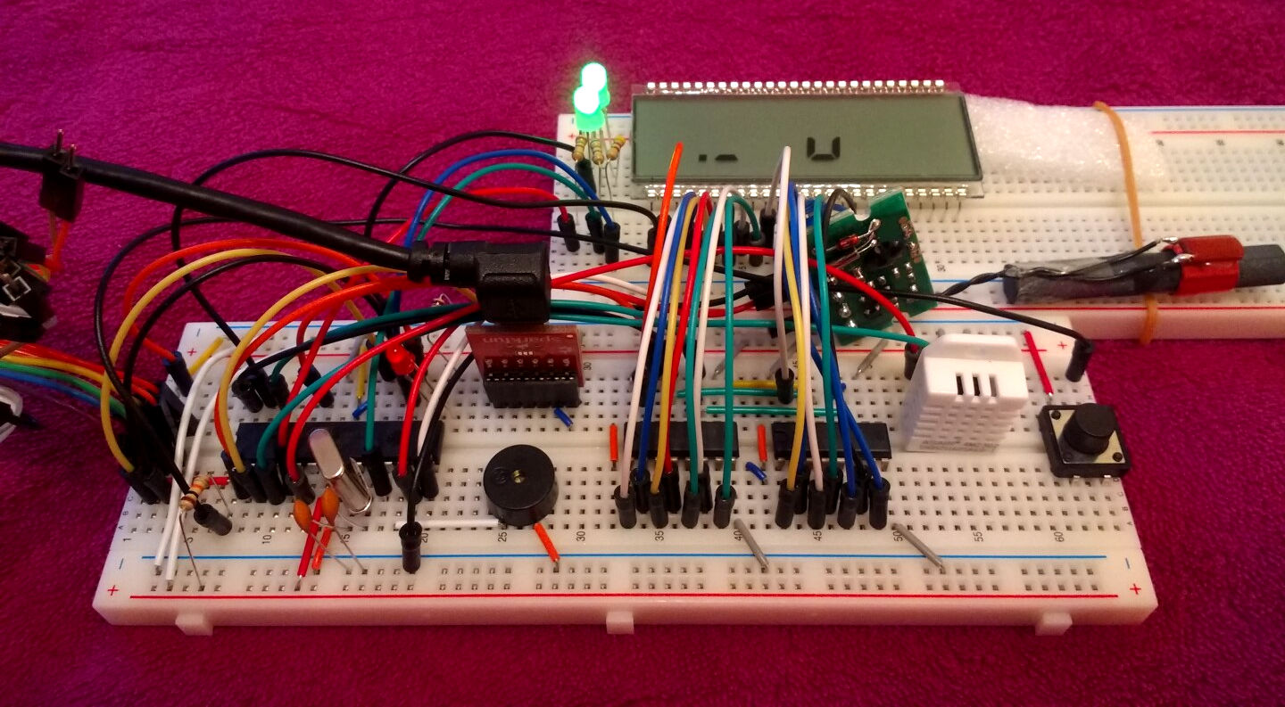
System PoC on breadboard (click to enlarge)
As you can see, I did not even bother to get all LCD segments connected up front, I just wanted to see if my chosen method of driving them worked before casting my ideas into a more permanent form (with a soldering iron). I stuffed two ‘595 shift registers on the breadboard (out of six total), implementing one LCD data line out of three. This allowed me to put up a binary counter and observe the segments change with various intervals.
The circuit
In the interest of lowering the power consumption, I reduced the CPU core frequency as much as possible. After some iterations, I settled on using a 2 MHz crystal with the CKDIV8 fuse programmed, yielding a core frequency of 250 kHz. This is well below the usual core frequency of 1 MHz and above (up to 16 MHz in the case of the ‘328P), and it did not come without challenges: I had to resort to counting instruction cycles and unrolling loops (trading code space for tighter execution timing) when implementing the DHT22 sensor interface.
But with a power supply of two AA batteries (providing about 3.2 V of supply voltage) the measured current draw of the system was a mere 50 μA! Assuming a battery capacity of 2,200 mAh yields a theoretical runtime of 44,000 hours, or roughly 5 years, but that is a bit optimistic as it neglects the power consumed by the shift registers, LCD module, and the occasionally powered sensors (not to mention the backlight). Still, it seems like a safe bet that I will not have to change batteries more often than every other year.
The input peripherals consist of three momentary push-buttons labeled MODE, SET and ADJ. I have come up with an elaborate scheme of how the menu system would look and work, but only a small part of it is implemented in software: pressing the MODE button cycles through displaying the time, the date, the day of week, the temperature and the humidity. You can press it once to nudge the display to the next “screen” or keep it pressed for slowly rotating them around. The backlight will softly turn on (with a ramp) and similarly ramp off after some seconds of inactivity.
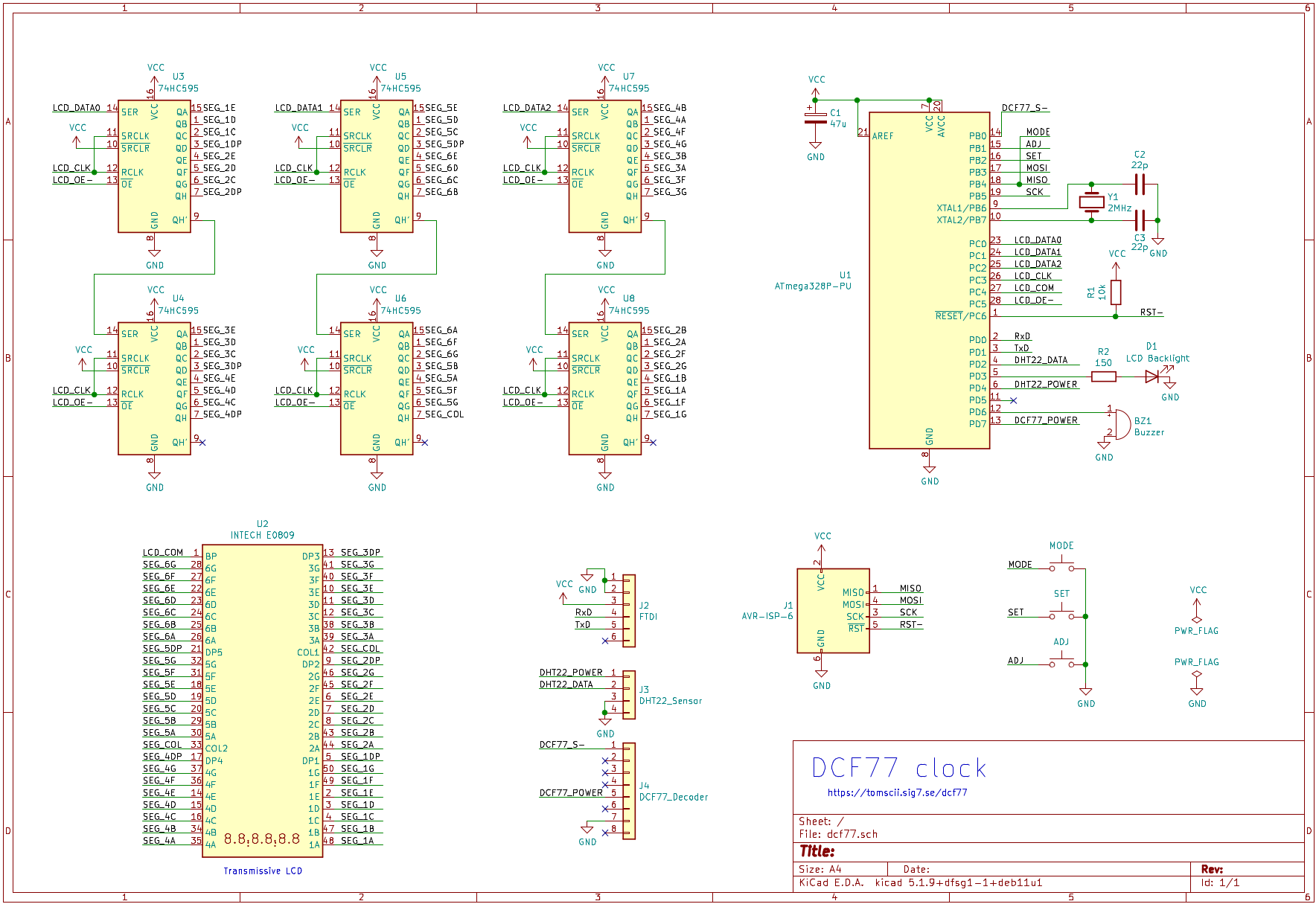
Below you can see the complete final schematic diagram of the central
unit, with connectors for the DCF77 receiver module as well as a
socket for the DHT22 temperature & humidity sensor (4 lines), plus an
FTDI cable connector (for the serial console) and finally the 6-pin
IDC socket for in-circuit programming the ‘328P. I de-soldered the
bulky screw terminals from the DCF77 module and connected its
double-spaced (200 mil) lines to an 8-pin standard 100-mil header,
feeding the negated output signal S- to the MCU input line.
Schematic (click to enlarge), PDF
I used KiCAD to draw the schematic – I found KiCAD to be an excellent choice given that it is free (GPLv3-licensed) software with great resources (tutorials and documentation) for new users while at the same time being powerful enough for professionals (or so I heard). I plan to get more into using it; learning the PCB designer and getting a real circuit board manufactured would be a great milestone forward in my electronic design abilities.
If you look closely at the schematic, you might notice that there is only a single LED providing backlight for the LCD, even though I promised an RGB backlight above. Well, it turned out that I could not procure a suitable RGB backlight, only a simple one with a white LED. So that is what made it into the final prototype. The software still has all the code for driving three PWM channels: red on OC2B (PD3), green on OC0B (PD5) and blue on OC2A (PB3). In the real circuit, only the red channel is used, along with the fourth PWM channel on OC0A (PD6) driving the piezo tweeter.
I came up with a custom electrical interface for the LCD. With 50 pins
(49 segments plus a common pin), we can’t directly attach the LCD to
the microcontroller – we need to arrange things so the MCU can
output individual segment bits in series. The 74HC595 CMOS 8-bit shift
register and driver is an ideal circuit for this. Deciding that we do
not want separate control of the two colons spares us one bit, so 48
bits fully define the LCD state. In the interest of speed, this is
divided into three lines of 16 bits, each line implemented by two
‘595s. The inputs of these shift register lines are called
LCD_DATA_0..2 on the schematic. With an additional three lines
(LCD_CLK for clocking, LCD_OE for shift register output gating,
and LCD_COM for the common pin), our LCD driver consumes six MCU
output pins and allows us to output 48 bits in 16 LCD_CLK periods.
Note that we need control of LCD_COM (consuming an output pin
instead of tying it to GND) so we can drive the LCD with an AC
signal. This is accomplished by alternating the phase of the outputs
while periodically refreshing the LCD: every second refresh, the
LCD_COM is driven high, and all data pins are driven active-low.
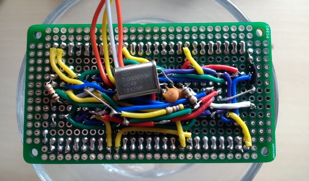
The prototype
After some rough planning of how to place the components, I started building the circuit on a 80x45 mm prototyping board. Because it is pretty much impossible to de-solder a DIP package (at least with a regular soldering iron) I opted for (crappy) sockets so I would not have to throw out the whole thing if I somehow managed to fry one of the chips.
In my infinite ignorance of how the RGB backlight would work, I soldered in two RGB LEDs under the LCD with the faint idea that they will “shine through” the semi-transparent LCD and thus create the backlight (I guess you can tell that I’m more of a software guy). Below you can see how it looked nearing completion, with all the ICs stuffed into their sockets (note the single rows of pin sockets for the LCD module near the top and bottom, and note that there is not a single free row in between them and all the IC sockets – this thing got dense):
Prototyping panel, front… (click to enlarge)
Above you can see the 6-pin AVR programming connection on the left edge. Due to the lack of an angled IDC socket, I just used a piece of standard dual-row right-angled pin headers, aligned to the board edge so the IDC plug’s notch would be blocked by the board when plugged the wrong way (the notch must be on the opposite side, above the board). Also note the piezo tweeter on the right of the board.
Unfortunately, using regular prototype wiring meant creating a rat’s nest on the back side:
…and back, some wires and connectors still missing (click to enlarge)
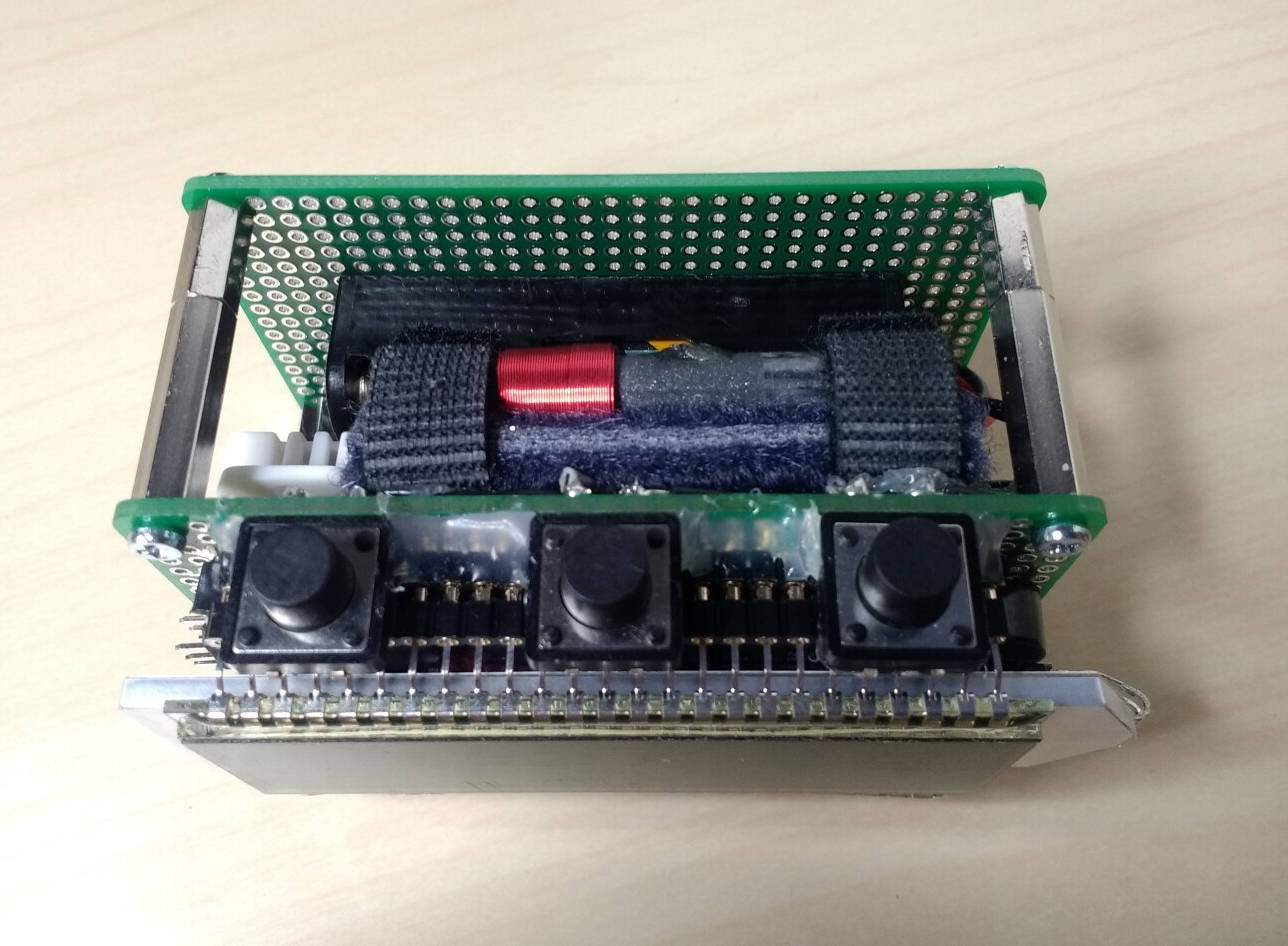
Somewhat miraculously, the device worked. Below is the finished circuit with both “daughter boards” connected (the DCF77 receiver on the left and the DHT22 sensor on the right, sitting in their respective sockets). In between them, the red JST RCY connector terminates the battery pack, making it easily removable.
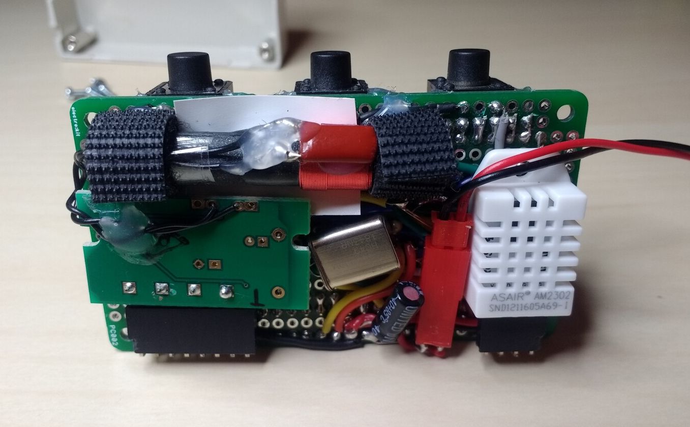
Prototype with DCF77 and DHT22 modules in place (click to enlarge)
I used some self-adhesive strips to form hooks holding the ferrite antenna in place, fastening the strips to the base board with some generously sized drops of hot glue. The PCB push-buttons also got their share of hot glue (I did not have proper right-angled buttons at hand; the planar ones I used had two out of four pins up in the air with the button’s side facing the base board, so it seemed wise to add some reinforcement there, even though the buttons’ bottom rests on the LCD connector).
On the angled view below, in the middle you can also see the FTDI header pins pointing towards the front side:

FTDI connector pin headers at mid-bottom (click to enlarge)
Magically, the above mess worked like a charm, and served as a stable platform for developing the software. I still won’t recommend this as a reliable way of building durable electronic circuits, and not only because it took a lot of work to connect all the wires…
Software
Most of the software is interrupt-driven, with a main loop that puts the MCU core to sleep after handling all events flagged by the interrupt service routines. This allows the ‘328P to spend most of its time in a low-power state. (Worth noting that besides well written software, achieving micropower operation requires extra care with the overall circuit as well. For example, a single output pin driven low while idle, with a 33 kΩ pull-up resistor on it, will drain 100 μA at a supply voltage of 3.3 V, blowing your complete power budget and more!)
Time-keeping and periodic operations (such as LCD refreshing) are driven by a TIMER1 overflow interrupt configured to trigger at 50 Hz. This 20 ms timeslice is called a jiffy, and time-keeping is based on counting jiffies. There is some clever code to compensate the crystal oscillator frequency with a correction factor between ±16 ppm (stored as a Q4.11 16-bit fixed point number, yielding an adjustment LSB of about 0.0005 ppm). Given the crystal’s rated tolerance, this range should probably be made coarser, but I got lucky with my crystal.
This correction factor is itself corrected each time a DCF77 timecode is successfully received, based on the difference between the received time and the local (internally kept) time, in proportion to the time since the previous such sync. The correction factor is saved to the device EEPROM, and even survives reflashing the MCU with new software. In my prototype, it ended up close to 6 ppm, compensating an error of about half a second per day (well within ±50 ppm, the rated precision of the HC49/U 2 MHz crystal).
In the interest of low power consumption, the external modules (DCF77
receiver and DHT22 sensor) are only powered on when actively used.
Exploiting their modest need of supply current and the relatively
strong drive capability of the ‘328P I/O pins, they are simply driven
by appointed output pins: DCF77_POWER and DHT22_POWER. Both
interface modules have a state
machine
to allow some wake-up time after power-on before the peripherals are
expected to work.
A DHT22 measurement will be taken periodically in the background once every 5 minutes (powering up and down the sensor each time), in the interest of maintaining a somewhat up-to-date value. I have some plans to extend the software with minimum/maximum display functionality (keeping track of the lowest/highest temperature and humidity since the last reset), which would necessitate ongoing measurements even when nobody is looking at the clock unit. In case the temperature or humidity screen is selected by the user (that is, displayed on the LCD), the five-minute measurement interval is reduced to 15 seconds. In this case, the sensor is continuously kept powered on until the user switches away from displaying the sensor results.
The DCF77 module will be powered on once per day (at 3 AM according to the local time) for a maximum stretch of a couple minutes, in order to receive a fresh time code. This is then used to update the local time as well as the crystal frequency correction factor (if necessary). This particular time of day (3 AM) is chosen for two reasons. First, this seems like a good time for receiving the DCF77 signal (at least at my location), as reception tends to be better during the night. Second, if there was a DST adjustment, this is the best time to pick it up. In case the device is powered on and there is no received time yet, the reception will be attempted immediately and then once every hour (until it succeeds). But if a 3 AM refresh failed, we will only retry one day later: the local oscillator, after having compensated the manufacturing inaccuracy of the crystal, is highly precise. Not receiving a fresh DCF77 signal for a couple days is no big deal.
The DCF77 reception algorithm is trivial, and is based on digital sampling of the DCF77 pin (only registering HIGH or LOW, 1 or 0) with a sampling frequency of 50 Hz (once per jiffy). First we establish bit-sync (“phase acquisition”) using a simple convolution filter aimed at detecting the exact jiffy (one in fifty) that is first in a second. Then we start sampling these DCF77-transmitted bits (AM signal with 0.2 s pulses for ‘one’ and 0.1 s pulses for ‘zero’) according to the bit-sync (“frame acquisition”), counting a pulse width of more than 7 jiffies (nominally 10) as a ‘one’ and more than 2 jiffies (nominally 5) as a ‘zero’. This is done until we have collected at least 60 bit samples and detect a minute mark (a one-second interval with no AM modulation, which we detect as a pulse of at most 2 jiffies to be noise-tolerant). On detecting a minute mark, we attempt to make sense of the last 60 bits we received according to the DCF77 time code, validating the parity bits. If validation fails, we continue receiving for another two minutes (at most) in the hope that we will have better luck.
If we have a successful reception, we compare it with our local time (if we have one, i.e., this is not the first sync) and do some sanity checks before we use the difference for crystal frequency compensation. Thus, we will not tamper with frequency compensation if the times are off by more than 5 minutes or if the date does not match what we believe is correct (maintained locally); if we have just crossed into a new year (where a possible leap second might throw us off – easier to discard this whole can of worms than to know for certain where those lie); or if there was a DST change (signalled within the DCF77 timecode). There are still plenty of nights when the local time-keeping oscillator stands to be fine-tuned.
The reception algorithm could be massively improved by exploiting that we know parts of the timecode from earlier attempts. Also, if this is not the first sync (we have a more or less precise locally-kept time) our a-priori knowledge of what time it is could be used to massively improve our decoding ability. This would be a nice tangent for people with advanced degrees in digital signal processing – while having some exposure, I sadly cannot claim to be one of them, but even I can imagine a vastly improved method. That said, the current trivial version (“zero-order approximation”) of the DCF77 decoder allows this cheap little receiver to correctly decode the time almost every night, keeping my clock exact (within the capabilities of a human observer).
First tests
With a minimally usable first version of the software up and running, I assembled the device, fastening the board into a fitting instrument box. Next up was the obligatory freezer test, which went without any issues:
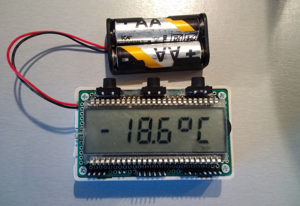
Fresh out of the freezer (click to enlarge)
Simulation
Continuing my software development activities, I quickly got tired of repeatedly flashing the device with the newest firmware (having to wait about a minute each time), oftentimes in rapid succession while trying to figure out some non-trivial piece of code by trial and error.
Looking around for an open source solution, I found
simavr, a cycle-accurate AVR
core simulator that can directly load the ELF executable file. This is
not the actual file that gets loaded into the MCU (that is a binary in
the HEX format), but the latter is derived from the ELF via an
avr-objcopy invocation, so the link between them is pretty
mechanical.
After spending some time with simavr (understanding the examples and browsing through its source code) I found it rather straightforward to build a full-blown simulator on top of it, implementing the bespoke hardware peripherals I used (programming their behaviour in some C coded modules) to complement the core. These modules interact with the I/O signals, so they can (and do) simulate complex peripherals like my custom-designed LCD output, the DCF77 receiver input and the DHT22 sensor.
Perhaps the biggest bonus of having a simulator (other than having a run-anywhere testbench without having access to the actual hardware) is observability. Not only can one look at any logical signal on the pins, one can also look into the processor (since all the internal state is computed) and look at register values. This can be extremely helpful, very much like using a debugger to look inside a running program, but for hardware.
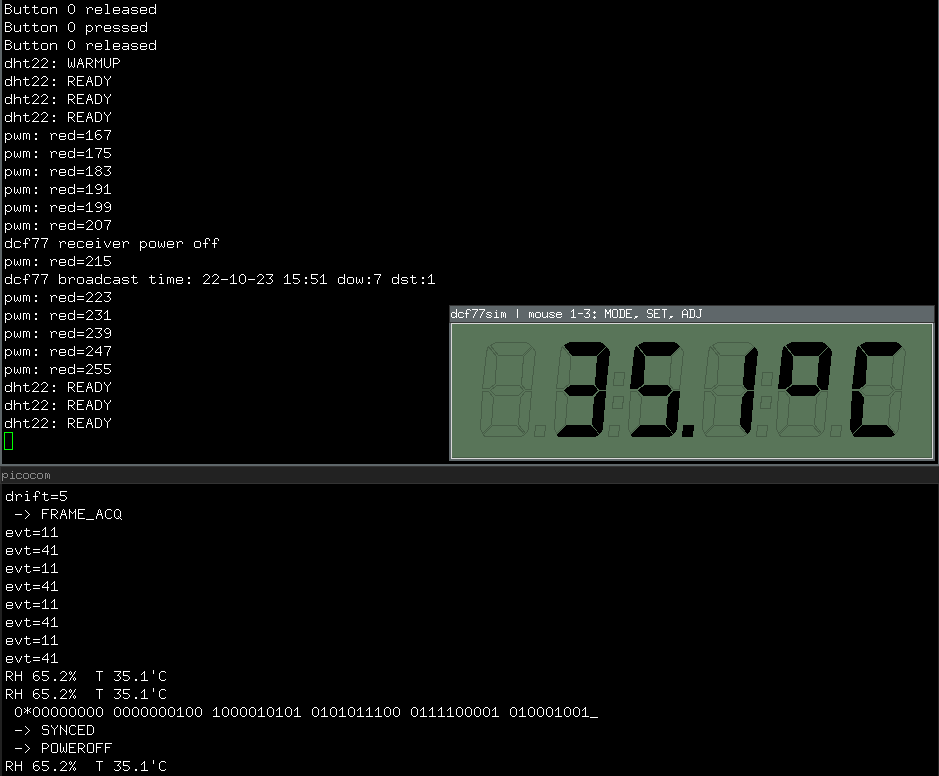
I used simavr in the usual manner, running my ELF code loaded into the simulator core (compiled with some extra debugging baked in, so not strictly identical to what goes into the hardware MCU, but very close) and saving a trace of selected signals into a VCD (value-change dump) file. This file is then visualized by any compatible tool; I used the readily available gtkwave.
The below image contains four traces of the LCD refresh cycle, in
increasing time resolution from top to bottom. For each cycle,
LCD_COM is either high or low, alternating from cycle to cycle. The
3 x 16 LCD_DATA bits (shown as a <Vector>) are shifted
out, clocked on the rising edge of LCD_CLK, at the start of each
cycle. (Every other cycle, when LCD_COM is high, these bits become
active-low and are inverted to convey the same meaning. An LCD segment
will be dark if the data bit is different from the common bit; in this
case, the LCD pin will sense a square-wave of ±Vcc with respect
to the common pin.) Finally, the active-low LCD_OE (output enable)
will be mostly low, only cut out for about half a millisecond while
the data is shifted into the ‘595 registers. Worth noting that the LCD
refresh cycle gets triggered by the TIMER1_OVF interrupt signal,
also traced out here (but not observable on any physical pin).
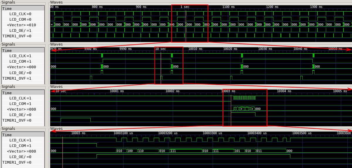
simavr: LCD refresh cycles (click to enlarge)
One can see how long it takes from the interrupt getting flagged
(rising edge of TIMER1_OVF) to the LCD getting serviced. Such
observations are extremely helpful in deciding how much code one can
squeeze into a certain recurring cycle, or if code needs to be
reshuffled to avoid blocking certain recurring operations. These
insights helped me time DHT sensor
readouts
(which use time-critical unrolled loops that must not be interrupted)
nicely interleaved with LCD updates, so neither gets disturbed by the
other.
Going further, I extended the simulator with a GUI: a window showing a graphical representation of the display, also capturing button events on the first three mouse buttons and relaying them as press and release events of the three physical pushbuttons (MODE, SET, ADJ) of the device. This allows the user to interact with the simulated device just like the real one. In the below screen capture, you can see this GUI together with two consoles: the upper terminal displaying the printouts of the simulator itself, and the lower terminal showing input from the (simulated) serial console of the device. It shows a trace of the last incoming DCF77 reception (60 bits in groups of ten bits), the last bit shown as an underscore (representing the minute mark).
simavr: GUI (click to enlarge)
The simulator generates a DCF input signal for the system according to the host computer’s current time, providing an end-to-end test of the receiver. (One can apply an offset to the current time, which makes it easy to test out boundary conditions such as a DST switchover.) On the other hand, the simulated DHT sensor encodes a hardcoded mock value on the wire (if I went all-in, I would probably use a real sensor and relay its data into the simulator).
The GUI accurately reflects the backlight in action as well (by virtue of a simulated peripheral device hooking into the PWM outputs, allowing us to alter the background color accordingly).
The simulator window is itself implemented as a very simple Wish (windowing shell) script, a.k.a. Tcl/Tk. It reads text from standard input line by line, carrying control updates to the display in a trivially simple format. Similarly, it outputs status on its standard output as notification of button events. You can probably see where this is going: the GUI process (the Wish interpreter running the GUI script) is run by the simulator core as an inferior process, connected to it via two pipes, one for the input and another for the output. I found this to be a nice and robust arrangement; if I started over, I would do the same thing again.
The simulator, essentially providing a full virtualized experience of running the embedded software on simulated hardware, was indispensable as I developed the finer parts of the menu system. It will no doubt prove its worth as I continue to implement more features. And it will be essential if I ever decide to take the receiver algorithm to the next level.
Improved construction
Now that I had much more capable software on board (developed with much help from the simulator described above), I wanted a more permanent, better enclosure. My first idea was to stick the battery pack on the backside of the box and call it a day. Alas, I had to discover that this destroyed the ability to receive the DCF77 signal; apparently, having that much metal so close to the ferrite antenna interfered with the signal. So I tore off the battery pack and reconsidered my options.
Meanwhile, I also researched how a proper LCD backlight module works, and decided to use one in place of the ill-advised RGB LEDs. I only found a simple white backlight module that resembled the proper size, so I reluctantly decided to use that, driven by the “red” PWM channel.
Finally, I settled on an improved mechanical construction with a second, identical prototyping board as the back side, holding the battery pack on its inner surface. The distance between the two prototyping boards is 30 mm, enough for the receiver to operate without interference. The full depth of the unit (from the LCD’s outer surface to the back panel) is about 50 mm.
Here is how it looks (click on any image to enlarge):

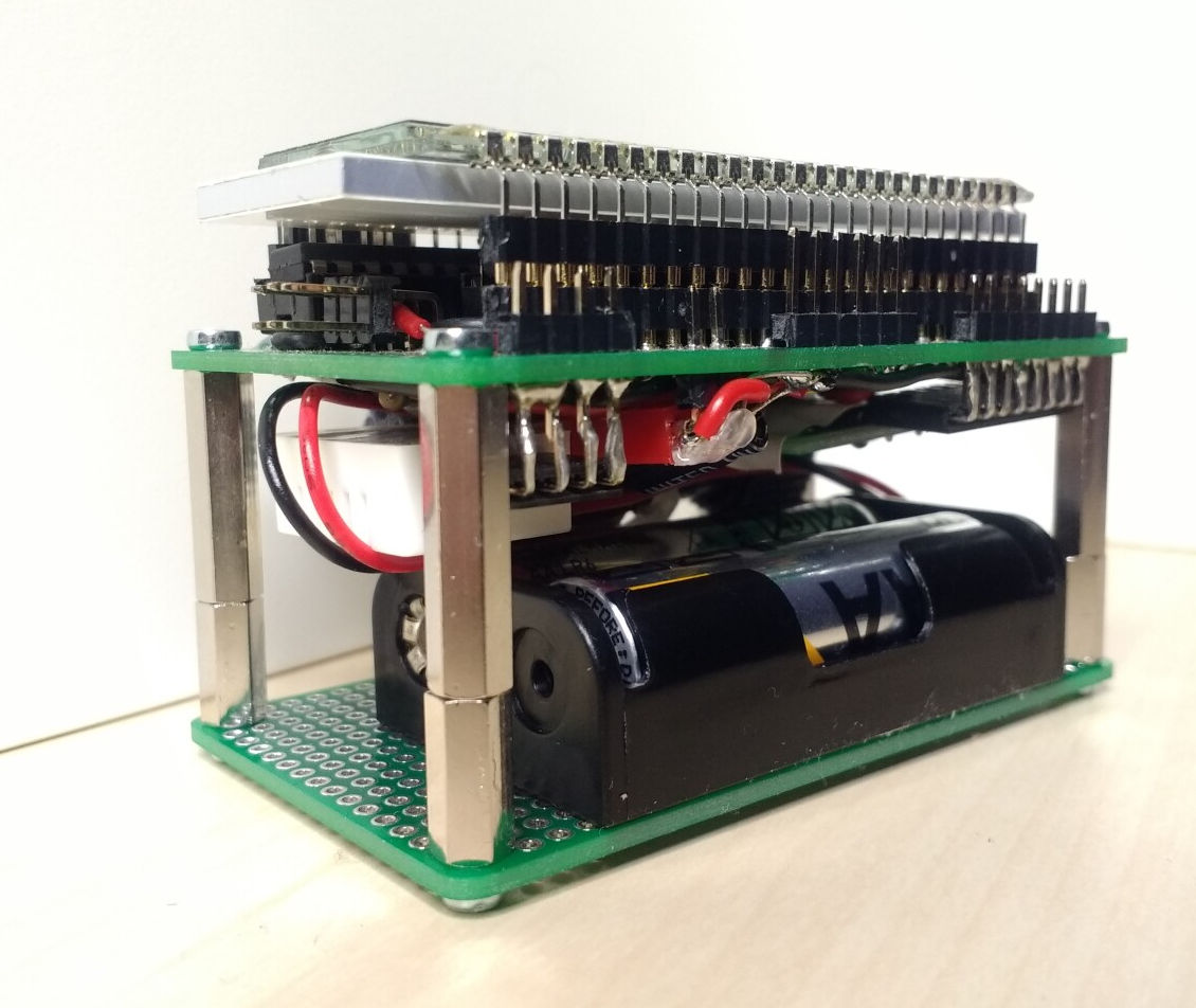
The backlight is a bit too wide; later on, I covered the protruding side edges with black insulation tape so as to mask all light but through the LCD.
Conclusion
The clock has been operational (in increasingly capable forms) for well over a year and a half now. It is still running on its first two AA batteries (as expected). It has successfully adjusted itself to all DST changes in its lifetime (all three, if I am not mistaken) and has always provided me with the exact time, something that microwave ovens are seemingly, and most irritatingly, incapable of.
Hardware cost and bill of materials
The cost of electronic components heavily depends on the purchased quantity: a single piece (if available at all) will be typically much more expensive (easily an order of magnitude or more!) than buying in bulk quantities of several hundred or thousand (depending on the manufacturer, type of component, distribution packaging of reel or box, etc).
The below table is therefore entirely for entertainment purposes and reflects how much I would pay my friendly local distributor should I newly buy, in single quantities, all the components built into this project. As indicated, these per-unit prices are insane compared to what you would pay if you set out to manufacture 10,000 clock units (and used a different distributor).
| Component | Unit price (SEK) | Quantity | Subtotal (SEK) |
|---|---|---|---|
| DCF77 receiver module | free (YMMV) | 1 | - |
| ATmega 328P-PU | 39.00 | 1 | 39.00 |
| 74HC595 | 5.90 | 6 | 35.40 |
| LCD 0.5” 6 figures, transmissive | 39.00 | 1 | 39.00 |
| Backlight for LCD | 25.00 | 1 | 25.00 |
| DHT22 sensor | 99.00 | 1 | 99.00 |
| Piezo tweeter | 15.00 | 1 | 15.00 |
| Crystal 2 MHz HC-49/U | 19.00 | 1 | 19.00 |
| Electrolytic cap 47μF 25V | 1.88 | 1 | 1.88 |
| Ceramic cap 22pF 50V | 1.20 | 2 | 2.40 |
| Resistor 150 Ω 0.25W 5% | 1.00 | 1 | 1.00 |
| Resistor 10 kΩ 0.25W 5% | 1.00 | 1 | 1.00 |
| PCB push-button 6x6x6mm | 5.50 | 3 | 16.50 |
| IDC male 6-pin connector, angled | 9.50 | 1 | 9.50 |
| 100 mil socket, 4 pins, angled | 9.00 | 1 | 9.00 |
| 100 mil socket, 8 pins, angled | 15.00 | 1 | 15.00 |
| 100 mil pin header, breakable, 40 pins | 9.00 | 1 | 9.00 |
| JST RCY male-female pair | 8.00 | 1 | 8.00 |
| Battery holder 2xAA | 9.00 | 1 | 9.00 |
| Prototyping board 80x45 mm | 38.00 | 2 | 76.00 |
| Metal distancer rod M2.5 15mm | 3.75 | 4 | 14.80 |
| Metal distancer screw M2.5 15mm | 5.50 | 4 | 22.00 |
| Screw M2.5 x 6 mm | 2.85 | 8 | 22.80 |
| Total: 489.28 |
We have almost reached 500 Swedish kronor, which is about the price for which you can get the cheapest ready-made DCF77-controlled clocks (without temperature/humidity sensing). However, I’d bet that this design could be manufactured in quantity for a per-unit component cost of at most 50 SEK (not sure about the DHT22 though, that looks a tad too expensive).
I have ommitted the IC sockets (I would not use them next time). Also, the DCF77 receiver unit seems to be out of stock, so I have not included a quote for that.
But of course one would also need to add to the above: the cost of wiring cables, cost of equipment (soldering station with assorted wire-cutting and trimming tools), and maybe most importantly, the (immaterial) costs of development (both hardware and software). I don’t think I’m going to start a business here…
Source code repo
You are welcome to check out the repository containing all the source code, simulator, hardware design and miscellaneous notes and documents I collected while working on this project. It is now shared online with all source code licensed under the terms of the very permissive BSD license.
You could in fact run the simulator on your own computer and play around with it, in case you are interested in how the clock works. And please feel free to take inspiration from it for your own projects.
The hardware design (KiCAD files) is also included in the published repository. Since I did not design a PCB up-front, it is more an after-the-fact documentation of the prototype that I actually built.
Still unimplemented features
Software is rarely ever really finished; rather, at some point you become satisfied with what it already does and accept any remaining shortcomings. That said, there are a couple things I have originally planned and still haven’t quite given up on yet. Especially with the simulator that I created for this project, further development of on-board software should be a breeze. Here is what I could imagine:
-
A stopwatch. It should have a start/stop button and a reset button (zeroing the current time) independent of each other. I want it to work this way particularly because of how I make pancakes – I like the timing to be accurate, and I want to be able to start a new run with a single press of a button.
-
Some good use for the second and third push-buttons (other than the stopwatch idea above). Right now it’s only the first button (MODE) that cycles through the available screens: time of day; date; day of week; temperature; humidity. (There is one “hidden” feature: holding down the MODE and ADJ buttons together for a couple seconds will trigger an immediate DCF77 reception. This is mostly useful for testing.)
-
The piezo tweeter is not used, ever. The hardware is there and the software contains the driver (it is even possible to toggle a whistle via the UART connection). There could be an alarm clock function. There could be some audible feedback on button presses. There could be cuckoo sounds synthesized on every hour. There are… possibilities.
-
A more scientific DCF77 reception algorithm (see below).
What I would do different next time
I had a lot of fun working on this project, but I also learned a lot of practical skills that I intend to use next time I do something like this. Here are some of my takeaways:
-
Design a real PCB and have it manufactured. Life is too short for hand-soldering wires to all the pins of a ‘328P, six ‘595s, and a 50-pin LCD, not to mention all the connectors. (And for all that hard work, the result is a sub-standard mess instead of a clean, neatly laid out, and silk-labeled circuit board!)
-
Consider using SPI for driving the ‘595s (all six daisy-chained). I already tested this method in another design with great success, and noted the benefits (less I/O pins; greater speed and less code without the bit-banging).
-
Put the DCF77 signal input on one of the ADC channels and use ADC readouts instead of digital input pin signals. This would allow a more sophisticated software-defined receiver based on digital convolution filtering. (Such a filter is used in its most trivial form to establish bit-sync, but as indicated above, the concept could be taken much further.)