De-smarting the Marshall Uxbridge
This is the story of a commercially unavailable stereo pair of the bi-amped Marshall Uxbridge, with custom-built replacement electronics: active filters feeding two linear power amps. Listening to this high-fidelity set has brought me immense enjoyment. Play a great album on these near-fields, and the result is close to pure magic! Over and above the accurate reproduction of a wide audio range, the precision and depth of its stereo imaging is stunning.
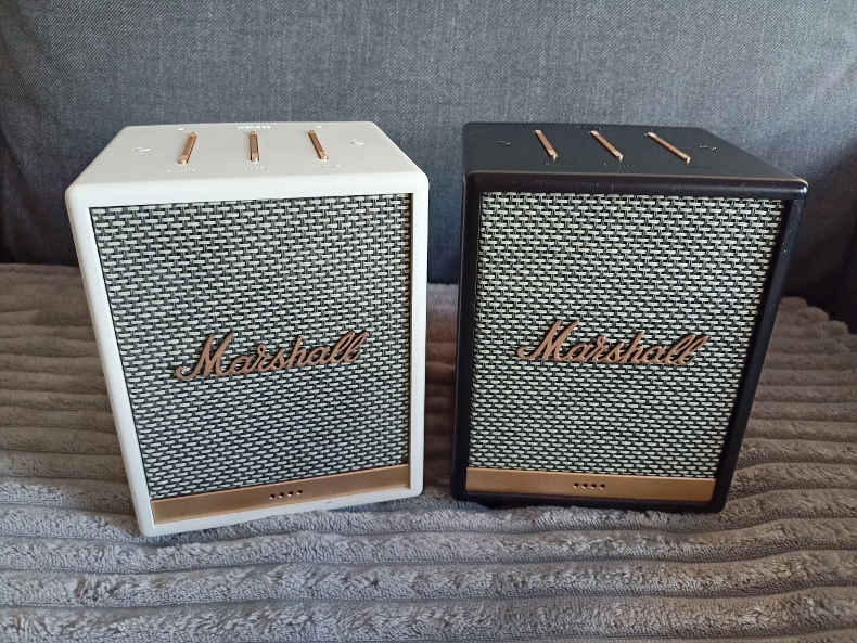
Odd socks, rock’n’roll! (click to enlarge)
Dumpster diving electronics is a way of life, which sometimes brings great moments of joy. One of these moments happened when I stumbled upon… the Marshall Uxbridge Voice, a smart speaker, in seemingly pristine condition. And not just one, but two of them! One was black, the other white. What a find!
What to do with these babies? Intrigued by the question “what could be wrong with them, why would someone throw them out like that?” – I set out to investigate. Plugging in one of them, after a few seconds of waiting, a female voice was heard: «NOW IN SETUP MODE. FOLLOW THE INSTRUCTIONS IN YOUR DEVICE’S COMPANION APP.»
Sounded like a command: clear, loud and demanding. But no, that won’t
happen. Instead, let’s see if we can use this gadget as a plain old
Bluetooth speaker? Yes indeed! With the help of blueman-manager, I
was able to hook it up to my Linux desktop (running Debian stable, as
ever) and select it as a speaker output. And it worked, and music
filled the room!
I was delighted, and immediately impressed by the sound quality. The low end was punchy and deep, much deeper than the modest dimensions led me to believe. The high end was crisp and detailed. Good drivers, I thought, and a good amp – there’s got to be some iron and copper inside, no wonder the thing is quite heavy! I liked it even though the sound reminded me of the “disco smile” (hollowed out mids), but I chalked that up to overly consumer-friendly default EQ settings. Maybe it can be improved.
The other device was similarly well functioning. I still could not believe my luck. Why would anyone throw out these excellent Bluetooth-enabled, powered speakers? They are doing such a great job!
Being in the market for a couple high-end speakers, I started to fantasize about making a stereo pair out of these two. Is that even possible? Probably not out of the box, as I could only Bluetooth-connect one at a time with the computer. While listening to a video, I also learned that the speaker added some 300ms of delay (compared to my wired headphones), which could be compensated, but was going to be a pain nevertheless. I had no idea if it came from the Bluetooth link or further processing in the “smart” speaker. Probably both. And any small differences between the latencies of two devices would certainly destroy the stereo imaging, if I ever got that to work…
Then the bland female voice suddenly came in over the music again, loud and clear: «CONNECTION UNSUCCESSFUL. CHECK YOUR APP FOR INSTRUCTIONS AND TRY AGAIN.» Oh my poor ears! And there goes my listening experience! Don’t you dare open your filthy mouth again!
At that moment I knew I was not into smart speakers. Or at least not into the smartness. The speakers were good. Oh, they were excellent! But they had to be de-smarted. Preferably with a single, dumb, analog RCA line input on their backs, so nobody but me gets to decide over the program material. That way I could also drive them as a stereo pair. No Bluetooth, no latency, no female robot overlord, just a good old-fashioned line input!
Seems like a modest ask. Can we have it? Well, time to look inside!
Inside the Uxbridge
Opening the enclosure by removing the backplate is a matter of pulling the six ordinary Phillips screws on the back. Then, the box can be pried open with some thin lever (screwdriver edge) – it fits snugly and is made even tighter with some air-tight foam.
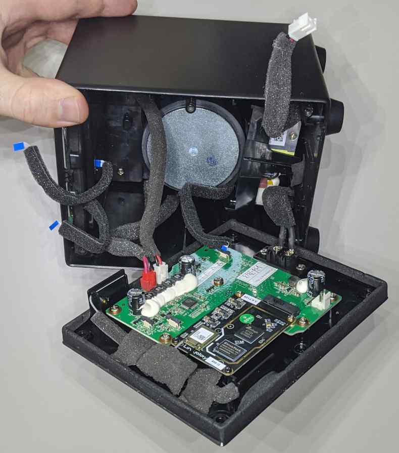
Original innards (click to enlarge)
The main electronics is on a board fastened to the back; it receives power from a separate PSU hidden under the woofer via the big JST plug (disconnected in the photo); the two smaller (connected) JST plugs connect to the woofer and tweeter (red and white, respectively). There are a couple flexible flat cables connecting to auxiliary boards hosting the volume and tone controls (plus the mics and push-buttons) on the top, and four RGB LEDs at the bottom of the front plate. I had to disconnect some of these, as well as the JST power plug, so as to take the above photo.
The main board comes with a smaller daughter board with Linkplay written on it. This is supposedly an OEM module for wireless connectivity and the “smarts” of the speaker: it contains an Amlogic A113X SoC, memory chips plus wireless module. The daughter board slides into an edge connector (not entirely unlike PCIe) on the main board. From the radio module, wires run off to two rectangular patch antennas fastened near opposite upper corners of the backplane. All wiring is covered in foam, and apparent care has been taken to make the enclosure air-tight.
The audio amplifier itself is built around an ESMT AD85050. This 48-pin device is apparently a knock-off of some class D power amplifiers, with rather scarce documentation of its own. It is employed in a two channel configuration, with separate power amplifiers dedicated to both drivers. These, both the tweeter and the woofer, measure close to 4Ω.
Looking at the circuit boards in some detail (and using a connectivity checker), it becomes apparent that the I2C control, the I2S two-channel digital audio stream and the 3.3V power all come from the daughter board. Which, unfortunately, is also the source of that vexing female robot commander voice.
Can we use the electronics? That depends on whether we are able to oust the resident voice of terror, and get hold of an analog input. Initially, I was hopeful, and felt that discarding everything between the PSU and the speakers, including a ready-made power amp already coupled to the speakers, would be a waste. As a first experiment, I removed the daughter board. Nothing worked – but in light of my earlier findings, I was not surprised. So then, assuming I cut the I2S lines to mute the damn robot, would it be possible to somehow inject an analog input to the (otherwise digital) amp?
With an “I’m feeling lucky” attitude, I somehow managed to solder some very thin wires connecting to the ESMT chip’s LINP, LINN and AGND lines in the hope of finding out. In case you were wondering, these are supposed to act as analog differential inputs for the power amplifier’s “left” channel (non-inverting and inverting, plus analog ground). As a first step, I tried asymetrically driving LINP (with LINN tied to ground). Nothing came out of the speaker; evidently, there is ample built-in fault-protection and shutdown mechanisms built into the ESMT chip to combat such abuse.
Next, using an op-amp on a breadboard, I attached a very temporary symmetrical driving circuit on the inputs. This did the trick of making sound come out, and it did sound pretty good (no obvious noise, distortion or interference), except that only the woofer was driven. Ah, of course! The tweeter is wired to the other (“right”) channel! So I would need to supply two symmetrical audio inputs to drive this amp. These would preferably be driven by an active loudspeaker filter circuit that limits the frequency range for each driver.
Considering the need for so many “patch” wires and the prospect of stuffing additional electronics into an already cramped box, this route seemed less than optimal. I also briefly played with the thought of keeping the digital-input amplifier; capturing the configuration sent to it via I2C and duplicating that from some microcontroller; then coming up with some way to drive the I2S digital audio input… somehow. Replace the daughter board? But too many unknowns remained, and I felt constrained by choices already made by others.
Going all-in
At the same time, the initially dismissed prospect of completely replacing the electronics started to look attractive. If I need to build a bunch of active filter circuits to separate the frequency bands before the power amps, sure I can add two power amps to that lot… and throw out the existing board! Which is not especially small, so there is plenty of real estate for its replacement.
And on the plus side, I could get rid of the idle power consumption of a full-blown embedded computer system (complete with Bluetooth/WiFi radio, so less EM pollution and potential interference), and less dissipated heat (I could sense the closed back of the idling Uxbridge get warm after half an hour or so). What’s not to like?
So let’s establish some requirements:
- The PSU supplies 18V DC. The whole system needs to be single-supply.
- Analog RCA line input on the back. Air-tight construction.
- Active pre-amp filter with the customary crossover of about 2 kHz.
- Possibly some further audio equalization / speaker compensation.
- Two power amplifiers, one for the woofer and one for the tweeter.
- Output impedance (both amps): 4Ω.
- Non-obvious thermal constraints: dissipation in a hermetically sealed box…?
- Obvious mechanical constraints (board size and JST connectors).
The first step in the circuit design (with the constraints on DC power input and speaker impedance set in place) was to find a suitable power amplifier architecture with actual, existing components. After very little searching, I settled on the LM1875T which seemed like a safe bet and promised high-end audio quality. The datasheet even has a reference circuit for single-supply operation.
Next, I decided on the crossover filters. Again, after a little reading up on this subject, I found no reason to search beyond the ubiquitous 4-th order Linkwitz-Riley filter architecture (two cascaded, identical Sallen-Key low-pass or high-pass filters to provide a steepness of 24 dB/octave) with the theoretical advantage of the channels neatly summing to 0 dB (in phase) throughout the crossover range.
What op-amp to use? I picked the LM833, not too expensive but quite capable with its 15 MHz gain-bandwidth, 7 V/μs slew rate and 4.5 nV/√Hz voltage noise. This is certainly a low noise, high speed op-amp when targeting the audio range, and as it is a dual op-amp, we can build a complete Linkwitz-Riley high-pass or low-pass filter out of a single piece.
The complete circuit
At this point, there is nothing left to do but draw the rest of the fucking owl, so that is exactly what I did. The complete schematic is available as a PDF; below I will highlight the functional blocks one by one.
At all times, keep in mind that we are building an analog circuit with op-amps, customarily fed with symmetrical supplies (with ground in the middle). Due to the existing power supply, we need to make the whole thing run from a single supply with respect to ground, and that is not how these circuits are usually drawn. It’s a technical detail, but an important one!
For this exact reason, let’s start with the virtual grounds for supporting single supply operation:

Virtual ground circuitry (click to enlarge)
We could be more fancy and use an active device (a dedicated “rail-splitter” like the TLE2426, or just a regular op-amp) to lower the source impedances driving these grounds, but in practice, given the tiny loads, a well bypassed, moderate impedance source will do just fine. With a non-obvious CAVEAT: For preserving adequate separation between the woofer and tweeter signal paths (or, rather, preventing cross-talk via the virtual ground), we use two separate virtual grounds, each dedicated to one signal path.
The single power rail VCC itself comes directly from the PSU connector J1; it supplies the three op-amps, each decoupled with a 100 nF poly capacitor:

Power input; op-amp supply & decoupling (click to enlarge)
These are sort of trivial details, and are customarily omitted when presenting analog circuits. It is important not to forget about them. With these out of the way, let’s look at the meatier parts of the circuit.
Active filters
The incoming signal is AC-coupled into the circuit via C1, after which R1 and R2 set the DC level to mid-supply (our virtual ground) for the signal to ride from there on. C2, together with R3 and the source impedance driving the line input, forms a first-order low-pass filter (fc ≈ 50 kHz assuming a source impedance of 600 Ω) to eliminate any RF interference just before the signal reaches the input follower U1A, which drives the rest of the filter circuits with low impedance.

Input buffer & active filter schematics (click to enlarge)
From here, the signal feeds two downstream signal paths. The upper one, built around U2B and U2A, consists of two cascaded Sallen-Key high-pass filters forming a 4-th order Linkwitz-Riley high-pass with 24 dB/octave steepness below its corner frequency. The passive component values are optimized to allow realisation with uniform values of commonly available high-quality polymer capacitors, and relatively small-value resistors in order to keep thermal noise contributions as low as feasible. This path ends in the signal TWR_IN, driving the tweeter’s power amplifier.
The lower signal path begins with a low-shelving filter around U1B, augmented with the divider-degenerating capacitor C7 to roll off DC response to unity. The purpose of this shelving filter is to provide emphasis towards the woofer’s lower end, in order to compensate its inevitable rolloff. The component values are the result of simulation and real-world tuning (as described below).
The bass-enhanced signal then goes through a Linkwitz-Riley low-pass filter (around U3A and U3B), a close counterpart to the tweeter HPF. Component values were guided by the same optimization criteria. The LPF comes last so as to attenuate the noise of preceding stages. The resulting signal WFR_IN drives the woofer’s power amplifier.
Note the nodes labeled VGNDT on R5 and R7: these are tied to a virtual ground dedicated to tweeter-side circuitry, set at half-supply. This ensures correct single-supply operation of U2B and U2A, as well as correct DC level on TWR_IN. In the woofer path, the equivalent circuit points can be tied to the real ground, as the DC level on the “cold” side of the capacitors C10 and C12 has no influence on the filter’s operation. The DC level on WFR_IN is determined by the R1/R2 divider right at the input; the whole signal path up to WFR_IN is DC-coupled (with a DC transfer of unity) from there.
SPICE simulation
To validate the above circuit, I first built a simulation model in the excellent XSchem, and asked ngspice to compute the frequency and phase response on both outputs.
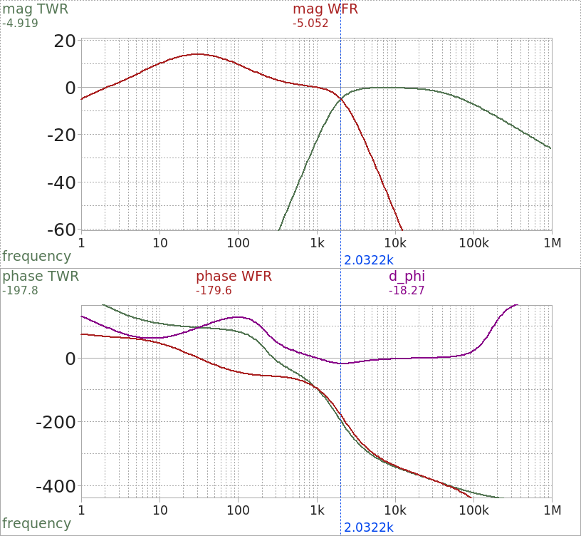
AC simulation: magnitude and phase response of filter outputs
The (electrical) crossover frequency is 2 kHz, with some slight bump in the summed output (as evidenced by each channel being a bit over -6 dB). The real (acoustical) response will, however, also be affected by driver response. According to listening tests, the woofer’s high-frequency roll-off roughly compensates the “electrical” bump in the crossover area.
What about the phase difference between the woofer and tweeter signal paths? According to SPICE, at the crossover frequency the tweeter output phase lags the woofer output by ~19°. That is equivalent to a delay of 19/360 times one cycle duration at 2 kHz, which works out to around 26 μs. Factoring in the speed of sound (340 m/s), this (electronic) delay is equivalent to an acoustic propagation path difference of about 9 mm.
In other words, the difference in signal propagation across the two filters is equivalent to the tweeter being 9 mm farther away from the listener than the woofer. In reality, the tweeter is going to be a bit closer to the listener, because the speakers will land on a table below head height, and the tweeter is mounted higher up in the enclosure. The exact geometry can vary quite a bit, but the geometric path difference will be in the ballpark – but with opposite sign!
As a consequence, the filter delay does not pose a problem; on the contrary, it might actually help the drivers’ sound waves arrive perfectly in-phase around the crossover frequency. Given the inexact nature of this problem (unknown variations in driver characteristics, plus the uncontrolled acoustic environment), we won’t bother with a delay compensator (allpass filter). It’s bound to be close to “perfect” anyway.
Power amplifiers
The power amps for the tweeter and woofer are principally identical, themselves closely following the single supply reference circuit in the LM1875T datasheet. The voltage gain is set to 10 (via R16/R15 and R20/R19), the lowest gain with guaranteed stability. A higher gain is not desired, because the line input would then become overly sensitive (its useful range, given the practical limitations on output volume, would be too low).
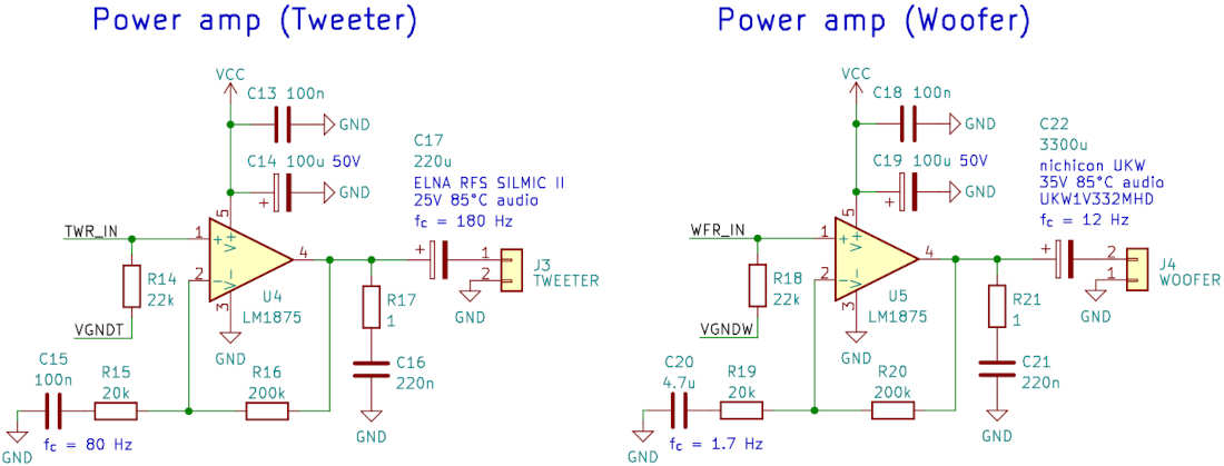
Power amplifier schematics (click to enlarge)
Between the amps, only capacitors differ in two positions. In both cases, we exploit the fact that the tweeter amp, given its useful frequency range, can get away with higher corner frequencies. The feedback loop degeneration caps C15 and C20 roll off the gain to unity at DC; here, C15 can be made significantly smaller than its counterpart. Similarly, the output coupling (DC-blocking) capacitors C17 and C22 form high-pass filters together with the load impedance, where we can again get away with a much higher corner frequency (smaller capacitance) in the tweeter amp. We do not max out this possibility (see the respective fc annotations), only to the extent that a significantly cheaper and smaller component can be used. We choose high-quality capacitors specifically intended for audio applications.
If you looked real close, you might have noticed one more discrepancy across the amps: opposite polarities of output connectors J3 and J4. That’s right, and reflect the fact that the Uxbridge driver cables have their JST connectors crimped with opposite polarities; however, both our amps are “straight” so one of them needs to have its output polarity reversed.
What kind of output power can we expect? The PSU just clears the lower end of the LM1875 supply range, so it’s going to be on the low end. The low driver impedance (4Ω) certainly helps a bit. Between the datasheet and some back of the envelope calculations, I expect about 5W of peak output power per driver (in practice, this applies to the woofer only; the tweeter will always be driven with much less power). That might seem low, but in practice, it is plenty for near-field listening in a quiet room. Thankfully, the low supply voltage also keeps dissipation down – a couple watts at most, and a mere fraction of a watt idling.
Prototyping and tuning
To validate the design in actual reality, I built a breadboard version of the complete circuit, from line input to the actual speakers. To ferret out any possible incompatibility, I powered it from the actual Uxbridge PSU removed from one of the units. This unit became my test harness: I removed the original electronics, extended the speaker wires and led them out via a small hole on the backplane (left in place of the Bluetooth button). I fastened the backplane in place and did my best to close the hole (with speaker wires protruding) using some tape. This way I could evaluate circuit performance with the real (non-ideal) speaker loads, together with real acoustics, and tune the filters after listening to music and pure sine tones. I was also able to A/B test, going back and forth between my circuit driving the prepared (closed) enclosure and the other complete, intact Uxbridge unit via Bluetooth.
I still haven’t built my first real DDS VFO / signal generator instrument (it’s in the pipeline, should be complete any year now…). For the time being, I reached for a “virtual” one by playing sine frequencies via online tone generators (first, second). I used them to establish general sanity, verify driver polarities, and equalize levels through the crossover range. I also tuned the woofer rolloff compensation filter with this method; I got satisfactory results down to about 35 Hz, which is on par with the original unit. The upper end? Limited by my hearing abilities… N.B.: All tuning and fiddling is already reflected in the circuits presented above.
Speaking of A/B tests: I also listened to lots of music, mostly assorted tracks and albums I enjoy and have been listening to all my life across a wide range of equipment and acoustic environments. I carefully compared the sound of the speakers; in a couple days, I reached the point where I preferred the sound of the new circuit. I believe it gives a flatter, more precise response especially in the midrange, where the original Uxbridge sounded hollow. I’m no fan of the “disco smile”; I prefer the mid to have some real bite.
Another reason I wanted a full prototype was to get a grip on the thermal situation. Having done those back of the envelope estimates, I was still quite uncertain about the amount of heat I could expect the LM1875’s to dissipate, and wanted to gauge heatsink temperatures (with the scientific “finger method”) both while idle and with realistic listening volumes. My estimates were validated; the TO-220 heating fins I planned for (and prototyped with) only got seriously warm at a loudness level I could not hope to sustain without creating “social problems”. Good, because there is not much point in putting a bigger heatsink into the air-tight enclosure…
Apart from the sorry fact that I was listening in mono (and in a bad way: only hearing one of the stereo channels!), everything seemed rather promising. Now comes the part which is, by now, a routine job: casting the circuit into permanent form by designing a professional PCB.
PCB design
This is a small-ish analog circuit, and we have plenty of real estate! We only need to match board size and hole patterns. We could go high-tech and use SMT components, and easily reduce the PCB area by a factor of two… but why bother? All the components are readily available, plugged into the breadboard. I would prefer to use them.
The complexity of this design is so low that the board is, in effect, single layer. Almost all wiring is on the component side, the rest of which is filled with a ground plane. The solder side is a complete ground plane (except a single, short copper bridge connecting VCC between C18 and C19). This double-sided, massive ground plane contributes to the low noise and high performance of this amplifier. A bunch of thermal vias under the heatsinks help the PCB take its part in spreading and dissipating heat.
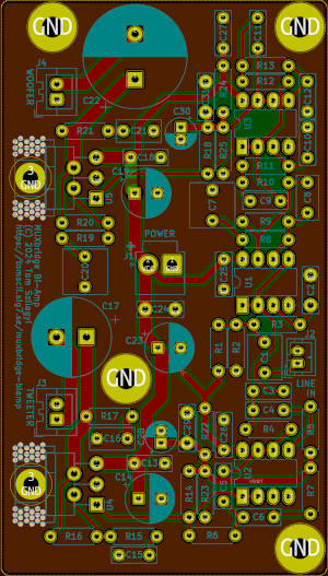
Printed circuit board (click to enlarge)
The dimensions are about half of the original panel – call me a dinosaur, but I see no need to design with SMT (requiring a stencil mask for applying the paste) to make it even smaller!
Below, a side-by-side comparison of the new dumb analog dinosaur and the original, fully digital smart technology:
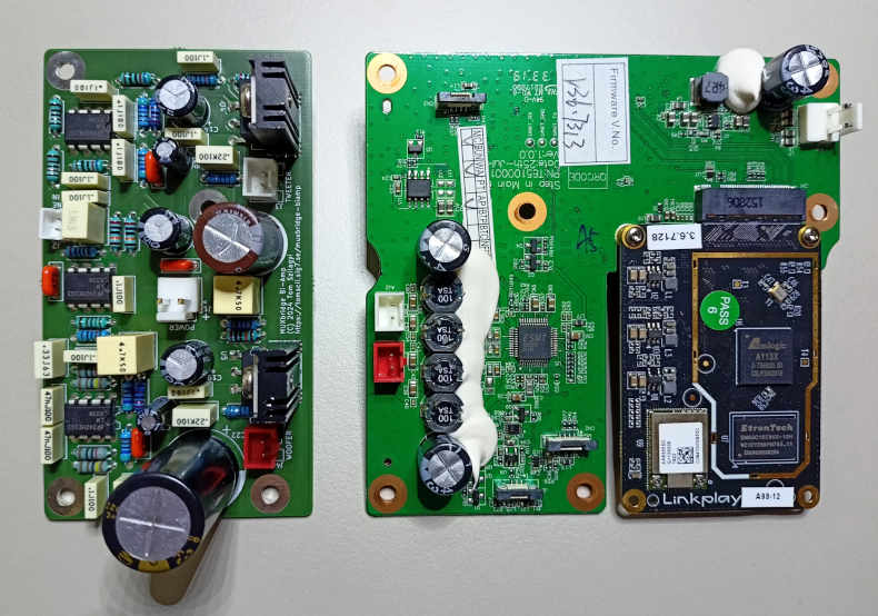
Electronics, new vs. old (click to enlarge)
Connectors and mechanics
Given the already crimped plugs on the PSU and speaker cables, I naturally wanted to keep the connectors on the new panel identical. The DC power connector was easily identified as JST-VH, and I had no trouble buying it. On the other hand, it took me some time to identify the speaker connectors as JST-XA. Worse, my local parts store did not carry it. The dimensions of the XA are rather similar to the more common JST-XH, except for the pin spacing (2.5 vs. 2.54 mm, not a big deal on a 2-pin connector). A more important detail is that the XH lacks the XA’s locking mechanism. In the end, I prototyped with XH (mating with the XA counterparts on the speaker wires). Eventually, I de-soldered the XA sockets from the original boards so I could solder them into my PCBs.
For the audio input, I picked a 2-pin JST-PH connector (2 mm pitch), using a matching plug with a pre-crimped short pair of wires. The bare ends were soldered to the female panel-mount RCA connector conveniently fastened into the backplane hole (⌀ = 6.5 mm) formerly occupied by the Bluetooth button. The back of the RCA connector was filled with hot glue to make it air-tight.
When the time has come to assemble my born-again speakers, it became clear that there was some obstacle preventing the back side from settling into place. At first, I feared the biggest capacitor (C22) colliding with the woofer magnet (during the design process, I convinced myself there was enough clearance, but now got the scare – my 3D skills suck!). Finally, it turned out that omitting the small cut-out on the board outline (visible on the left edge of the original panel) was a mistake. That space was taken by the plastic stem receiving the middle-left Phillips screw (looking from behind the box). The issue is clearly visible in the below photo (look at the middle hole along the left edge):
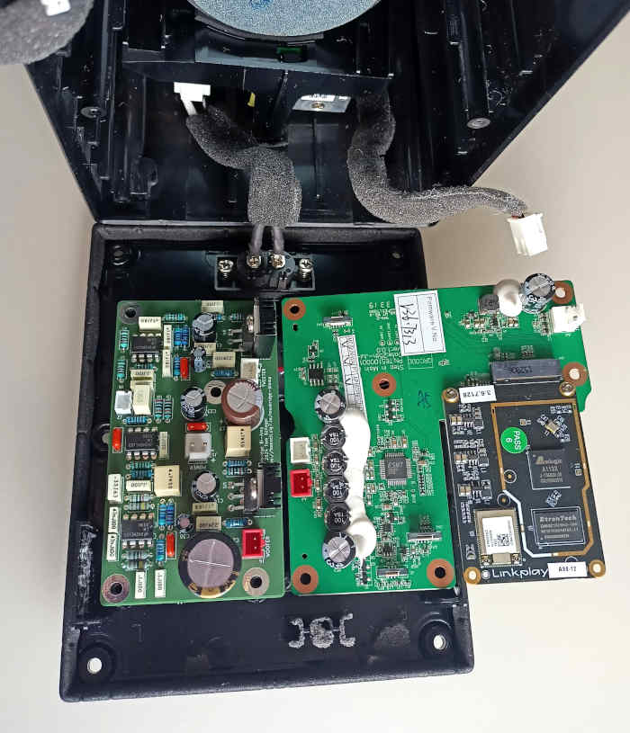
New panel in its place: can you spot the bug? (click to enlarge)
Another image of the second unit, exhibiting the same issue.
Well, out with the rasping set! I managed to remove just enough material (about 2 mm) from the plastic stem down to the required depth to make space for the PCB edge. Plastic filings carefully vacuumed out of the box. Success, with footnotes (there are always footnotes)!
Conclusion
In the past several weeks, I listened and re-listened to many of my long-time favourite albums and all I can say is, I absolutely love the sound of this pair of odd socks! The listening experience is on par with, or easily surpasses, any stereo I ever had (and I’ve had a few). Even though I don’t have the means to measure, in the first hours of listening I felt a dramatic step up in fidelity from the original Uxbridge. I am convinced that tuning the active filters with the speakers in the loop has given me a superior frequency response, and the linear power amps at low power are likely to have less noise and distortion. The sharp stereo imaging is another sign of high fidelity. The fact that I got these “from the bin” for free (at least the enclosures, power supplies and drivers) gives me a smile each time I turn them on.
It appears that analog electronics in the audio range is more or less a solved problem: discounting the obvious extremities of high power (hundreds of watts) or really miniscule signal levels (microvolts), it is not too difficult to create, with contemporary semiconductors, a simple circuit charting seriously audiophile territory!
As always, the sources of this article (in this case, the KiCAD hardware design plus XSchem workspace and ngspice simulation files) are published online with everything licensed under the terms of the very permissive MIT license.
Update: This article has been discussed on
Hacker News.