Taming the buck with a Type III compensator
I recently designed and built my first DC/DC converter, a synchronous buck regulating some hefty DC currents. It turned out to work okay-ish (except the overvoltage crowbar), but I had a nagging feeling that it could (and should) be improved further.
Even though the prototype made it through a testing regime of load currents (up to the full rated load of 5A) effected via mechanical switches without self-destructing, one thing that kept bothering me was the substantial ringing in response to a modest 1A load step.
For simplicity (and because I believed it would provide sufficient stability) I have originally used a Type II compensator in my design. I won’t reproduce the compensator network and its simulation here; please take a look at my recent article in case you missed it.
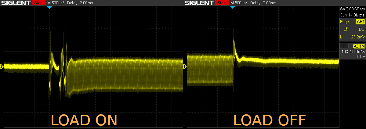
The measured real-life step response of that design (switching on and off a resistive 1A load) was captured as below (reproduced from the previous article):
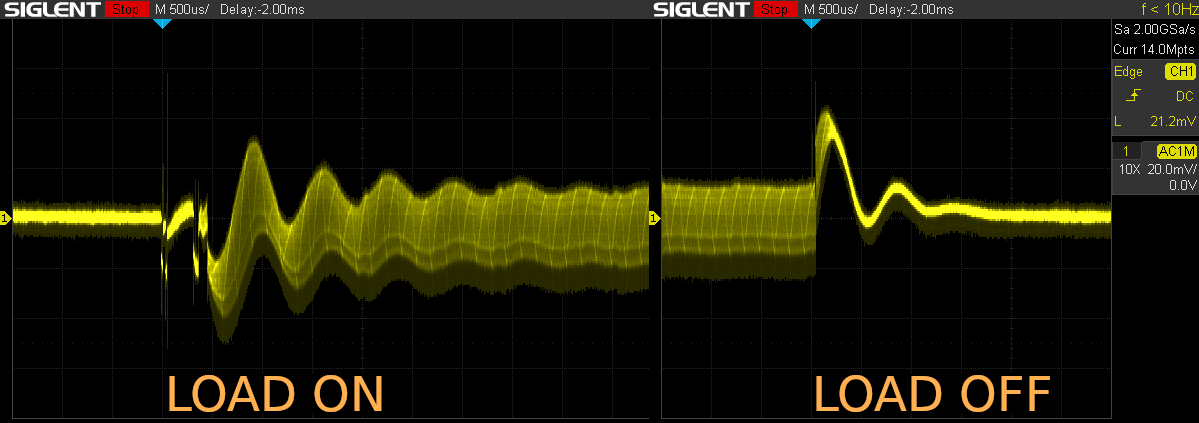
Load transients with Type II compensator (click to enlarge)
It’s definitely stable in the sense that ringing does not turn into a self-sustained oscillation. But it’s pretty ugly! Control theorists would probably say that the phase margin of the control loop is insufficient. They would also add that the stability of said loop might possibly only be conditional – meaning that under the “right” conditions (load impedances), there could be oscillation. With bad, potentially catastrophic, consequences.
I looked again at this wonderful document called Technical Brief 417 (local copy) I studied previously and made the belated discovery that I probably needed a Type III, rather than a Type II, compensation network. In hindsight, it’s a bit unclear why certain facts were not plain obvious at the time, but digesting the material once more, everything clicked.
But to check myself, I first decided to improve on my SPICE simulation. It became clear that my rendering of the phase margin has been insufficient, or rather, nonexistent, as I have not even produced a graph of aggregate phase response, only looked at the controlled system (the LC filter) and the compensation network in separation. So first things first, below is the simulated bode plot showing the closed loop response of the original Type II compensator:
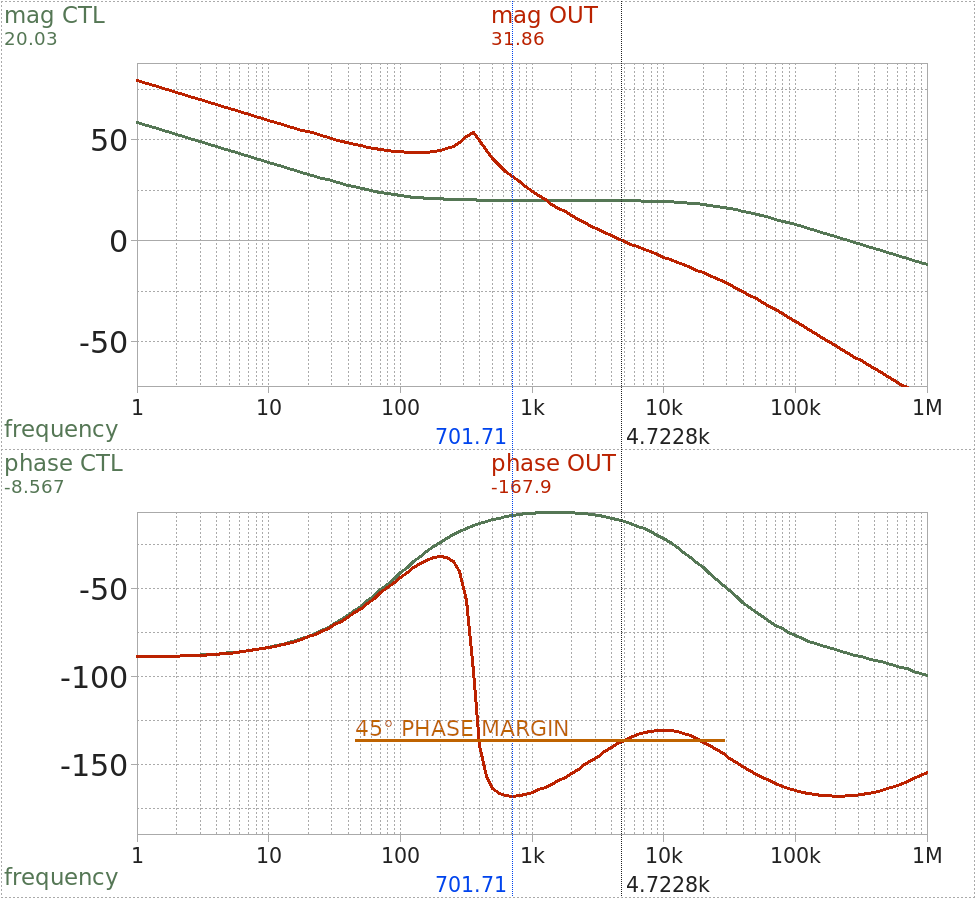
Closed loop response with Type II compensator
The green line (CTL) is the response of the compensation network by itself (as shown previously); the red line (OUT) is the same, plus the response of the LC filter (also shown by itself, previously) in the aggregate. And naturally, it is this aggregate response of the whole closed loop that counts when judging stability.
Note: I have subtracted 180° (inverting input of the error amplifier) from the closed loop phase shift, as usual. The remaining phase shift, if it reaches 180° with the gain still above 0 dB, will combine with the 180° due to negative feedback to produce positive feedback, and therefore oscillation. How far we are from this point is called phase margin.
It is known that a phase margin of at least 45° is desirable for an unconditionally stable closed loop. I have hand-drawn the line corresponding to this margin, and the calculated phase response quite obviously violates it: at its peak around 700 Hz, there is 168° of phase shift (so only 12° margin), dangerously close to the limit. Also note that the closed loop bandwidth is only 4.7 kHz (the loop gain crosses 0 dB there). That is a bit lower than I would have liked – 10-20% of the 100 kHz switching frequency would be ideal.
Can we do better?
Well, not with the Type II compensation network! Notice that the response of this network by itself (CTL) peaks in its phase response in the same area where the closed loop phase margin is the worst. So we have already tuned the compensator as well as is practical.
Hence, Type III compensation, which adds not 90°, but 180° of theoretical phase boost! And the best part is, it’s all the same circuit, just with an added resistor and capacitor. So I can easily test it for real using my existing prototype!
Here, let me show you the updated model:
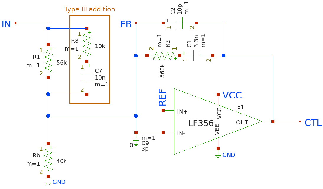
Type III compensation network model
It is, as promised, almost identical to the Type II network presented in my earlier article. New components are marked as Type III additions. Everything else is exactly the same.
And the calculated response (as above, compensator only in green, closed loop in red):
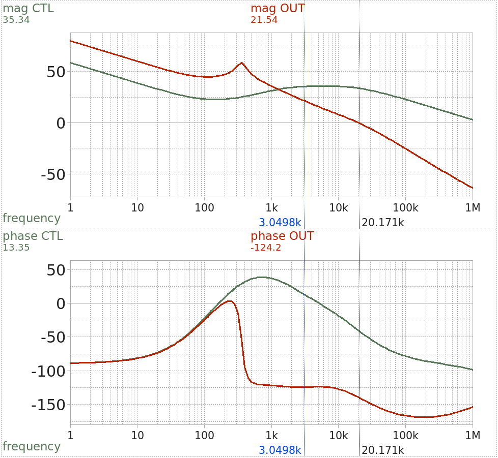
Closed loop response with Type III compensator
Now we’re talking! One obvious improvement is the hugely improved phase margin: it hovers around 60° (barely touching 55° at 3 kHz), forming a wide plateau between 300 Hz and 10 kHz. Meanwhile, bandwidth has improved to 20 kHz, which is perfect! Not only has stability improved, but the system also reacts faster (responsive at higher frequencies). This is noteworthy insofar as increasing stability usually means giving up bandwidth, moving poles down in frequency for increased damping…
Only one final question remains: how much is all this nifty theory worth in practice?
A poly capacitor and metal oxide resistor soldered to the underside of the prototype PCB, Manhattan-style on the divider upper leg 56 kΩ resistor’s leads, is all it takes to find out!
Using identical settings to my original measurements, the below load transients were produced and captured in short order:
Load transients with Type III compensator (click to enlarge)
Do scroll up and compare that closely with the image at the top of this article. (In any sensible browser, control-clicking here and here will open both in separate browser tabs. Then you can easily switch back and forth between them.) It’s really worth the effort!
The mechanical switch bounce at “load on” looks the same. But the similarity ends there – in fact, there is hardly any ringing left to speak of. That validates our estimation of a phase margin close to 60°. A bit less, to be sure, but close.
Well, at least there is some slight transient. Below is the “load off” transient with 10x horizontal zoom (50 μs/div):
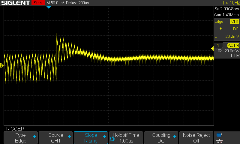
Regarding the very pronounced shift in ramp amplitude, I speculated in my original article about this being caused by the non-linear magnetics of the filter inductor. With that out of the way, the only thing of interest here is the envelope transient, with a peak of 25 mV. The inductor bias current seems to decay in ~70 μs; there is hardly any action after ~200 μs.
And that is what I’d expect from a well designed control loop!
Footnote: I originally had some trouble with XSchem, trying to plot a phase response beyond the usual range of ±180°. As a result of an AC simulation, ngspice produces a complex vector. The magnitude and phase of the bode diagram come from this vector, with phase computed modulo ±π radians. For systems with multiple poles and zeros, that translates to abrupt jumps across those extremes, which makes for an ugly and confusing graph.
Within the realm of ngspice, this
is solved by the function cph() (continuous phase) that takes care
to return a phase vector without these jumps (adding or subtracting
2π as needed to keep the graph continuous). I discovered that
there was no equivalent XSchem built-in. So I opened xschem issue
#238 and to my
delight, Stefan responded with an implementation of the missing
cph() function… committed and pushed to master within less than an
hour! With XSchem, Stefan has very tangibly contributed to my SPICE
simulation abilities that lie behind this article, and for that I am
most grateful.