Synchronous buck converter for 12V/5A output
What is the logical next step after making a linear regulator? I learned some valuable lessons (both regarding general electronics and power supplies) doing that project, so I believe I could now make a much better linear supply. And perhaps I will! But now I decided it was time to aim for a switch-mode power supply (SMPS), a.k.a DC/DC converter.
This article documents my take on a synchronous buck regulator for outputting 12V at currents up to 5A, from an input voltage that is nominally 48V, but in practice can be between 15V and 55V. This circuit is my original design, so I will go into a lot of detail on how it works, and share ample measurement data around its performance and efficiency.
But first, I present you with a photo of the finished prototype (alas, both heat-sinked MOSFETs are hiding behind the toroidal inductor):
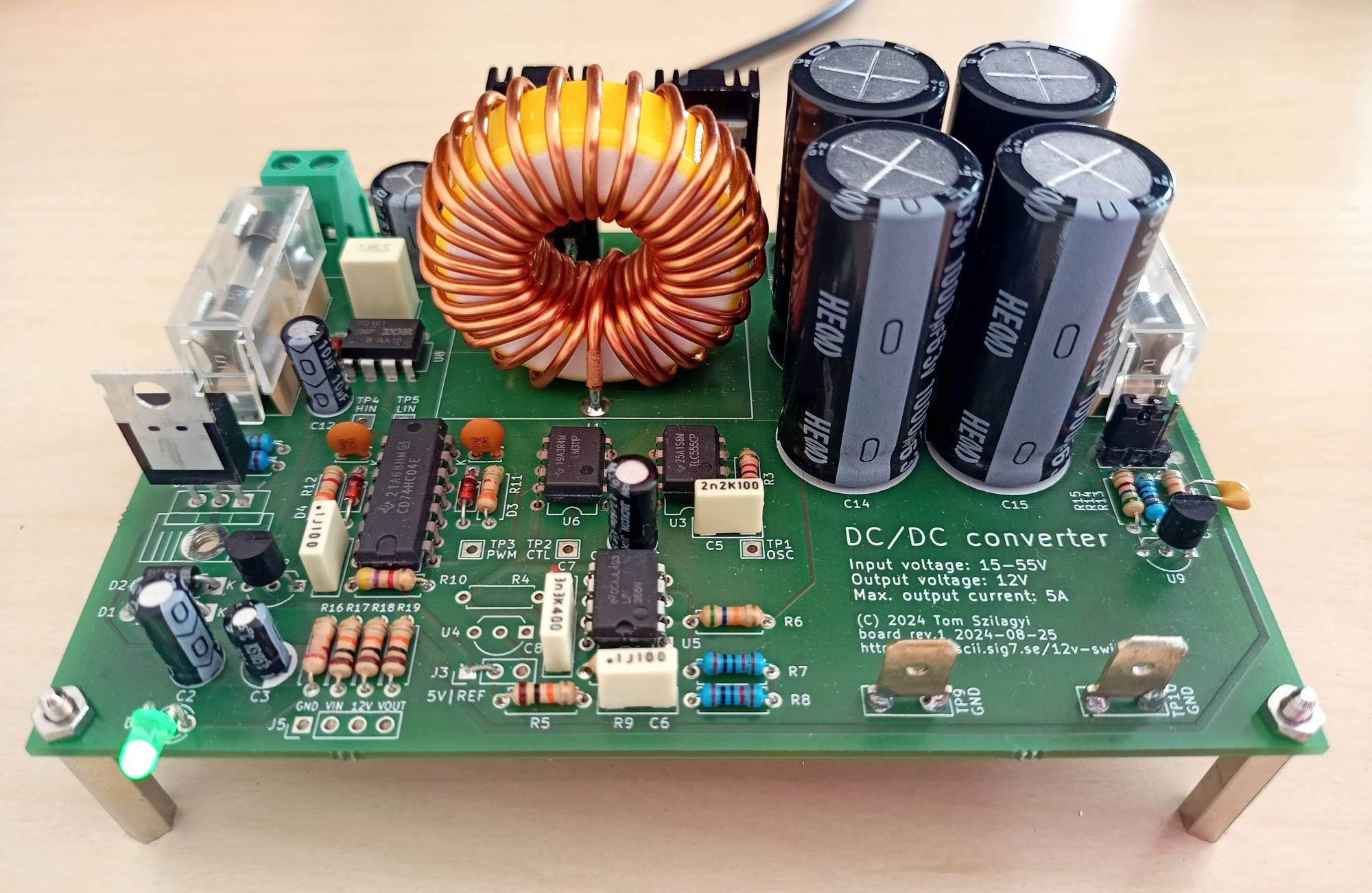
Buck converter prototype (click to enlarge)
The motivation for designing and building this device was two-fold. First, I wanted to get practical experience designing a switch-mode power supply myself, getting acquainted with all the tradeoffs and pitfalls of the design space. I find that I only really understand technology that I can also build myself (to some usable standard; not necessarily state of the art). And switchers are everywhere; this tech absolutely dominates contemporary power conversion. So I naturally wanted to have it under my belt. Alas, textbooks only get you so far – I have spent many frustrating hours trying to understand arcane but important details that are simply not very well exposed (or totally omitted) in popular books teaching electronics.
The second reason for this particular device: I am planning to build a UPS (a project of larger scope, with multiple electronics modules) for protecting my self-hosted “data center” at home (hosting this very website and my source code, among other things). My plan is to have a DC UPS inserted between the 12V supplied by the power brick and the computing hardware (Synology DiskStation plus networking equipment), also outputting 5V power for the small ARM SBC hosting Internet-facing web services. The battery backup for this is going to be a hefty Li-Ion battery of nominally 48V (originally for electrical bikes) that I conveniently have at hand; later I might swap that out for something else. Hence the design criteria for the switcher presented below. Stay tuned for future articles describing additional parts of this DC UPS system.
Features
- Nominal input voltage: 48V (can be between 15V and 55V).
- Output voltage regulated to 12V.
- Maximum rated output current: 5A.
- Over-current protection provided by fuses on both input and output.
- Resilient in the face of an output short circuit: fuse blows, MOSFET does not.
- Monitoring outputs for connection to the rest of the DC UPS system.
- Voltage-feedback PWM control loop at a fixed switching frequency of approx. 100 kHz.
- Synchronous buck topology yielding very high efficiency (~94% as measured).
- Low output ripple (roughly proportional to load current; about 70 mV peak-to-peak at full load).
- Load transient response: output transient peak less than 50 mV at 1A load step; settling time ~1 ms (Improved compensator: ~25 mV peak; settling time ~200 μs).
A final note on this project: Why am I wasting my time building a switcher from the ground up, using generic components (no bespoke switcher IC) instead of just building a proven reference design around some well-known switcher such as the LM2575 (which comes in versions for fixed as well as adjustable voltages)? Well, part of it is curiosity and the desire to really understand what makes a switch regulator work (and ideally, work well). But an equally important aspect is that commercially available ready-made integrated switchers either do not offer output currents as high as 5A, or do not tolerate input voltages as high as 55V. And I need both.
Operating principle
If you have any level of familiarity with switch-mode power supplies, the below block diagram is probably nothing new:
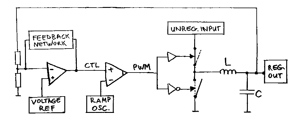
Synchronous converter block diagram, napkin-style
To make a synchronous buck converter, a PWM control signal is used to drive the switching devices in a complementary fashion. These switches, of which only one is active at any given moment, either drive the output LC filter with the unregulated input, or shunt it to ground. The cycle is periodically repeated at the switching frequency. At a first approximation, the output voltage equals the input voltage times the duty cycle (ratio of ON-time to the total cycle time).
To make a voltage regulator out of this buck converter, we feed back a fraction of the output and compare it to a fixed voltage reference. This is done by the error amplifier, which outputs a control signal that in turn gets compared to a ramp (triangle wave) signal running at the switcher frequency. The comparator generates a PWM signal with a duty cycle proportional to the amplitude of the control signal. The PWM and its negated version drive the switches. The closed control loop ensures that the output will assume its nominal voltage, and stay there regardless of changes in supply and load.
That is the one minute elevator pitch you usually get by looking at introductory material (such as the general treatment in electronics textbooks). Digging deeper (in books dedicated to power electronics), you find… complexity. Control theory filled with obtuse mathematics and all sorts of obfuscated formalisms to treat the subject. I have developed a deep-seated conviction that most of it is unnecessary. But at least some of that complexity is legitimate, because switchers are prone to all kinds of misbehaviour unless carefully designed.
Some of the more subtle points at play:
- The two switches (almost always power MOSFETs operated as saturated switches) must never be on at the same time. To avoid this, switcher control circuits usually include some dead time between switching off one transistor and switching on the other. This ensures that there is no shoot-through transient current while both transistors are (partially) conductive.
- Proper driving of power MOSFETs is a whole topic in itself. The designer needs to get acquainted with concepts like total gate charge (required to effect a switch transition) as well as arrange for the right voltage levels: the gate of the upper side N-channel FET must be raised well above the input voltage, which is the highest conveniently available voltage in the system. (Using a P-channel high side switch has its own issues.)
- Not only that, but power MOSFETs are notoriously easily destroyed by a less than perfect circuit – it’s enough to momentarily exceed their gate-source or drain-source breakdown voltages, with catastrophic device failure as the (almost certain) result. Most often, additional protection circuitry is needed to arrive at a robust circuit. How that protection interferes with normal operation is left as an exercise to the designer…
- The control loop must have a tailored frequency response that blends well with the LC output filter. Control theory is like an iceberg (there is much more of it and it goes deeper than you would prefer). In practice, this means a frequency-dependent feedback network closing the loop around the error amplifier. It is important to get this right, or else nasty loads can cause serious mischief – oscillations, self-destruction, madness and depression.
- It is wise to think long and hard about transient states in addition to the more easily digestible “steady state” of the whole system. What if things are out of balance? What happens when the thing is suddenly turned on (with all capacitors at zero charge)? Hint: a controlled slow start is desirable at all but the lowest power levels.
It should be clear by now that power electronics is not for the faint of heart. It is a field of endeavour much like an arctic expedition: mistakes of judgment tend to be fatal. I knew that the road to a robust switcher design would be paved with dead MOSFETs, so what I did up front was improve my SPICE skills to have a fighting chance with a circuit that might actually work, even if practice will inevitably force revisions of the theoretically perfect design.
SPICE simulations
After some time spent evaluating contenders, I found XSchem to be an excellent playground for circuit dilettantes like myself. I have previously used “naked” ngspice only (i.e., wrote a netlist by hand and ran ngspice from a terminal, with some extra gnuplotting at times).
Contrary to my initial fears, I found XSchem to be very usable, easy to learn and well worth the time investment. I could finally draw a circuit and quickly simulate it, then change component values and iterate… a much nicer workflow! Although it took me quite some time to grasp all the possibilities of setting up simulation graphs right in the XSchem schematic, adding computed data series with custom formulas, and so on…
XSchem is great, but it is only a frontend to ngspice, so I still spent countless hours fiddling with component models and fighting the ever-so-frustrating “timestep too small” errors… and I think I might have finally developed a working skill of solving the most egregious convergence issues in a SPICE simulation. (Sssh, don’t tell anyone!)
LC output filter
Every design needs to start somewhere, and the design of this switcher started with the inductor. I chose a 50 μH toroidal inductor, nice and big, rated for 10A max current, with a specified copper resistance of 16 mΩ. Why? Because the next smaller one was rated for 5A (too small) and based on the already chunky size, I dared not move up to an even higher inductance. But based on switcher IC datasheets and reference designs, I believed 50 μH would be enough to make a good switcher.
Okay, next up: switching frequency and filter capacitance. I chose 100 kHz for simplicity (switchers customarily operate between 50 kHz and a couple hundred kHz). I wanted to keep it somewhat on the low side to have more leeway driving hefty MOSFETs. With this parameter also set, the required filter capacitance is driven purely by how much we want to constrain the inevitable output ripple. Here I dreamt big and used some bulky caps that might seem like overkill: 4 x 1000 μF (promising a low ESR of 45 mΩ at 100 kHz) in parallel. That will work out to about ±20 mV of output ripple, a comfortably clean output by switcher standards.
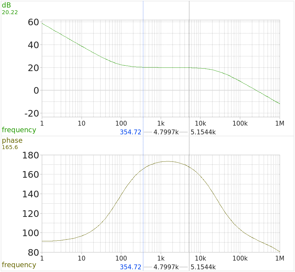
This leads us to the below SPICE model and AC simulation results of the LC filter:
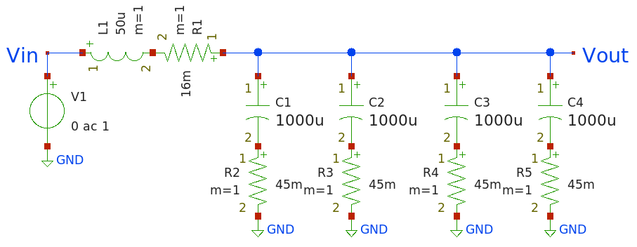
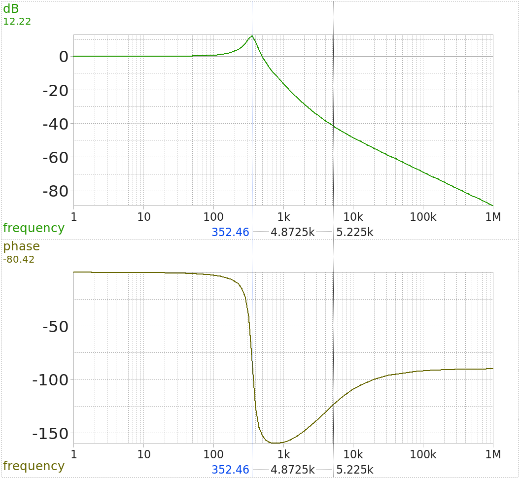
LC filter model and its AC simulation
As expected, there is a peaking resonance (as in any plain old LC tank). The peak is 12 dB at around 350 Hz. A second breakpoint (due to capacitance ESR) is visible at a couple kHz. But we should not take these figures too seriously – the model data might be grossly inaccurate, and it is completely without parasitics. We probably underestimate both inductances and resistances.
Error amp with compensation network
On the most basic level, the control signal (CTL on the block diagram) is proportional to the desired output voltage. If the control voltage goes up, the PWM duty cycle will also go up, which will result in a higher output voltage. So it might seem like all we need is a proportional control in the feedback loop: straight amplification of the error (deviation from the desired output voltage).
The problem is that we have completely neglected the dynamic behaviour of our system. The LC tank is prone to oscillations at its frequency of resonance, and as a result our controlled system will behave in an extremely suboptimal (possibly catastrophic!) way in the face of load transients. We need to design the controller taking the system’s dynamic properties into account. In other words, we must design the control loop in the frequency domain.
As we already have a frequency-domain model of the system to control, designing the optimal control loop is (in theory) a solved problem. If we know enough control theory. (Hint: we don’t.) Fortunately enough, there is a wonderful document from Renesas, affectionately titled Technical Brief 417 (local copy). This is the most accessible, no-nonsense treatment of the topic I was able to find. I highly recommend that you read it carefully if you are interested in the subject. I will not reiterate any details of the design procedure found there, only summarize my takeaway:
We need a Type II compensation network. This feedback network (to be connected between the inverting input and the output of the error amplifier) is made up of a single capacitor in parallel with a series RC. It makes the error amplifier’s transfer function assume a certain (desirable) shape in the frequency domain. Sizing of the parts should be done so that the corner frequencies are approximately correct. The result of this exercise is a closed control loop with guaranteed stability, with near-optimal transient response. That’s it!
Referring you once more to the Renesas document if you are at all interested in the details, here I only present you with the SPICE model and AC simulation results of the compensation network I came up with:
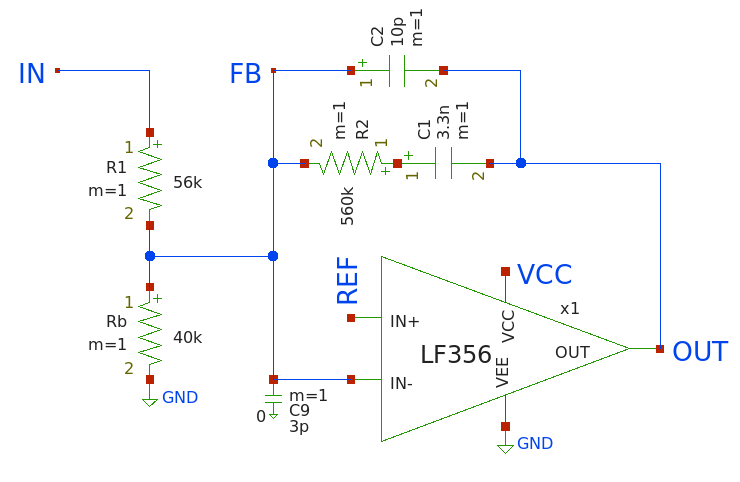
Type II compensation network model and its AC simulation
The input of this network assumes a 5V voltage reference. The resistors in the divider are relatively large, so as to not draw too much current. I am probably being overly conservative here, especially given that this necessitates an even larger resistor in the feedback path (to secure the +20dB mid-band gain). The 3 pF cap on the inverting input represents parasitics, and helps SPICE avoid convergence errors.
You might wonder why I built this with a jellybean generic op-amp, the JFET-input LF356. You won’t see such a thing in “real-world” designs – it’s either going to be part of an integrated switcher control chip, or they use a TL431. However, I thought it would be an interesting exercise to realize all functions of the switcher with generic parts. And the LF356, while not over the top, is a pretty nice op-amp with a gain-bandwidth of 5 MHz, which feels just right. It is also quite cheap. Well, not as cheap as a single TL431, but two or three.
The cursors in the AC simulation are set to the corner frequencies from the LC tank simulation. As apparent, this network provides close to 90 degrees of phase boost in that range, which is required for stability. The lower breakpoint of the compensation network could possibly be lower and the mid-band gain increased; there is probably room for future adjustment here – but I’d like those to be based on real measurements, not simulations!
[Update: read my follow-up article on upgrading this to a Type III compensator, and the improvements brought by that change.]
Complete regulator
With the above pieces at hand, we can create a SPICE model of our complete regulator! That’s right, we can (with some judicious simplifications) create a model of the closed control loop and run transient simulations with it to validate its behaviour. In theory, of course.
Without any further ado, the model:
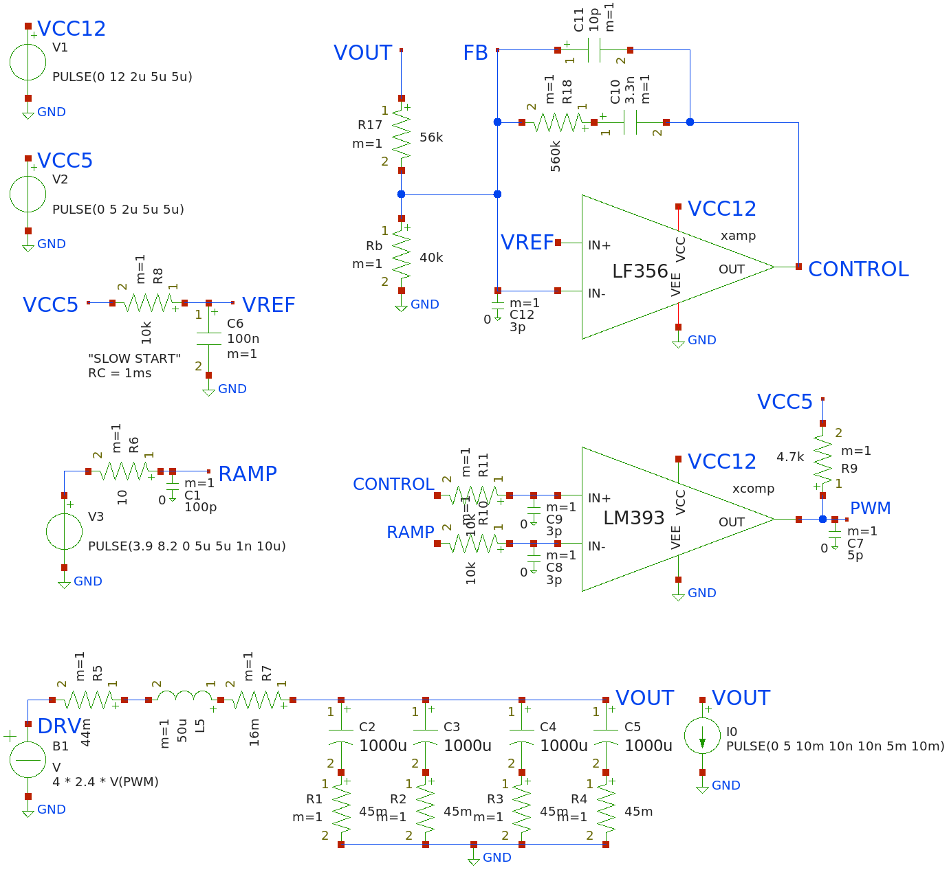
Complete regulator model (closed loop)
A quick rundown of its parts:
- Voltage sources on the left: 12V and 5V supplies (initial ramp-up helps SPICE find its way without needing tedious explicit initial conditions).
- Reference voltage derived from 5V supply via a “slow start” RC divider.
- Ramp generator. Finite (nonzero) source impedance and some parasitic capacitance is generally a good idea to help with SPICE convergence.
- Upper right: Error amplifier with Type II compensation (as already presented above).
- PWM generator based on LM393 voltage comparator (because it has an easy to understand, simple SPICE model, and it’s good enough). Several sacrificial (imaginary) components to appease the SPICE god. The output pull-up resistor is real; we pull up to 5V because that logic level will feed the (unmodeled, actual) MOSFET driver.
- Output driver (bottom): based on a B-source, this forces a voltage on DRV that is 4 x 2.4 x PWM. The multiplications make 12V out of an 5V logic-level input (2.4x), then 48V out of the 12V (4x). So the source is 48V while PWM is high (5V) and 0V while PWM is low (0V). The 44 mΩ resistor models the ON-resistance of the switching device. The rest is the LC-filter model (as already presented above).
- Finally (bottom right), we have a pulsed current source forcing step load currents on the output: 5A on/off every 5 ms, after an initial waiting time of 10 ms to allow turn-on transients to settle.
As you can see, there are no MOSFETs in this model. We therefore do not need any MOSFET drivers either and can also do without a dead time generator. All this means less trouble with convergence errors, and much faster simulations! (How do I know that? Do not ask…)
Despite the omissions, this simplified model is still quite capable of simulating the overall dynamic behaviour of our control loop, which is probably the hardest aspect to get right. Some characteristic simulation results:
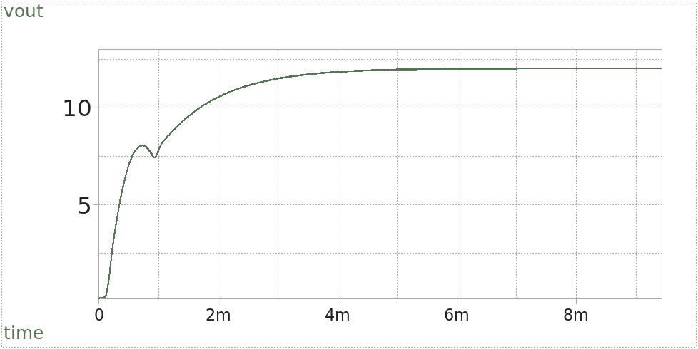
Time-domain simulation: Turn-on slow start
The gradual ramp-up of output voltage is quite close to the theoretical RC charging waveform with a 1 ms time constant. That is exactly the voltage reference of the error amplifier, and apart from a small bump around 1 ms into the rise, our regulator follows faithfully. After 5RC, the output voltage is very near its final value of 12V, as predicted by basic electronics theory. And importantly, there is absolutely no overshoot above the nominal output voltage.
Let’s zoom in heavily on both scales and inspect the output ripple. Not only that, but the load transients as well (both ON and OFF) on a composite image:
Time-domain simulation: Output ripple; Load transients
In line with basic switcher theory, SPICE reports an output ripple of approx. 20 mVpp, independent of load current. Switching on the 5A load causes a downward-peaking output transient of about 60 mV and settling in ~200 μs without any serious ringing. Switching back to idle results in a very similar (but inverted) transient.
There is a lot of fun to be had (and many more hours merrily spent) tweaking circuit parameters and inspecting their effect on the simulated behaviour. But the above seems pretty close to ideal!
The real circuit
Equipped with the above simulations, it’s time to design a real circuit we can build and test. Below I present the functional blocks one by one, in logical order. The complete one-page schematic is available as a PDF if you prefer to take it all at once. (There are some additional notes on the sheet that I am omitting below, such as measured current consumption of all the blocks. Knock yourself out.)
12V and 5V supplies
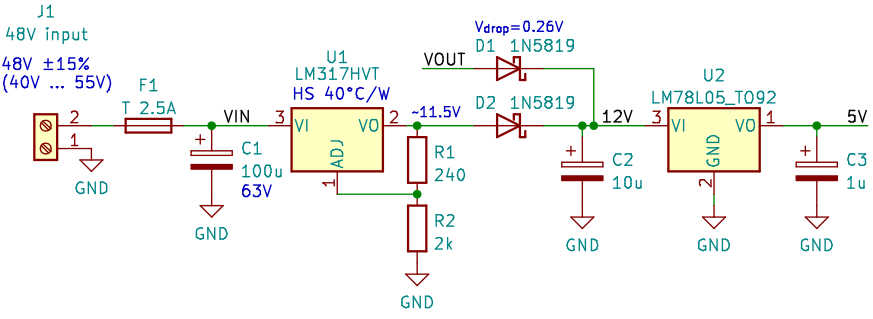
We use a high voltage variant of the ever-popular LM317 to bootstrap the circuit’s 12V supply. After the regulator is up and running, we will be using the regulated output VOUT to feed the regulator itself. The Schottky diodes D1 and D2 make this dual-supply a safe proposition. We aim for a slightly lower voltage at the output of U1, so the regulator output will “win” and relieve the inefficient linear supply.
The heatsink on U1 is therefore completely unnecessary, unless we decide to not do this self-feeding by omitting D1 (and perhaps substituting D2 with a jumper wire). In that case the heatsink will be mandatory… and warm!
VIN is the unregulated supply for the whole circuit, hence the relatively large electrolytic buffer. The fuse is sized for 48V input; in case of running full load at lower input voltages, it needs to be raised appropriately.
Error amplifier
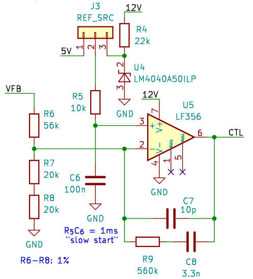
VFB is the voltage feedback from the output, principally identical to VOUT (but taken before the output fuse). The precision shunt regulator U4, together with R4, supply the 5V reference voltage. Alternatively, if greater precision is of no concern, these two parts can be left unpopulated and the reference taken directly from the 5V regulator. Connector J3 has a 2-pin jumper on it, shorting one of the side pins to the middle pin to select the source.
The reference voltage source feeds the “slow start” RC (R5, C6) just as in the SPICE model. The Type II compensation network is also identical. CTL, the output of this block, controls the output voltage via the PWM generator.
Ramp oscillator & PWM generator
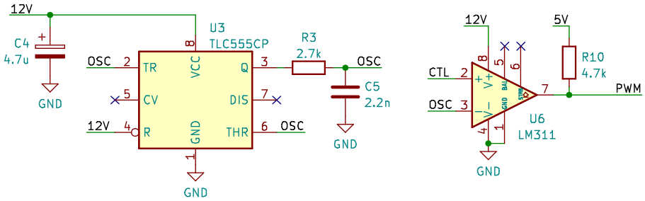
After experimenting with some fancier op-amp based relaxation oscillators, I went back to the basics and chose this oscillator based on a CMOS 555. Its ramp voltage is not linear, but RC-exponential (as expected). That does not really matter to us; the important thing is that varying the comparator threshold will yield a smooth control of the PWM duty cycle all the way from 0 to 100%. That necessitates sharp edges at the turns of the ramp, which the 555 provides with ease (unlike other circuits I have tested). The only gotcha with the 555 is the need for a relatively large bypass (C4) to achieve transient-free switching, even with the supposedly low current CMOS variant.
For the PWM generating comparator I used the LM311 in the actual design. It is 3x as fast as the LM393 in the SPICE simulation (~200 ns vs ~600 ns response time), and comes as a single device per package (with offset adjustment possibility) with an uncommitted output transistor, but is otherwise quite similar. It’s an upgrade at no additional cost.
Above are the actual measured waveforms OSC (yellow) and PWM (pink). The ramp oscillates between 3.9V and 8.2V with a frequency of approx. 106 kHz. (Previously, I showed you a SPICE model already back-annotated to accurately reflect this amplitude range. This is an important detail, as it determines CTL’s range of effective control.)
The PWM signal has fast falling edges (as expected) and more leisurely rising edges due to the much higher drive impedance. We could lower the pull-up resistor value for sure, but we would be wasting power, and it does not really matter – the edges are already plenty fast for the buffered inputs of the 74HC04 inverters driven by them.
Dead time generator
Now for something new I left out of the SPICE simulation! (I did simulate it separately, but kept it out of the main model for speedier runs.)
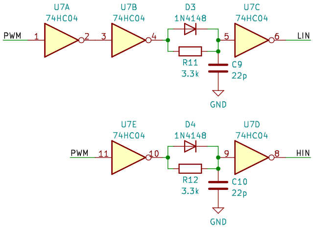
The dead time generator is built with a hex inverter of 74HC logic, hence the 5V logic level output of the PWM generator. And the 5V regulator. We could possibly use some high voltage CMOS part here (such as a 4049 or 4069) and do away with the 5V supply (mandating the use of the precision shunt for the error amp reference voltage), but I chose to go with something I had previous experience with. Enough unknowns already!
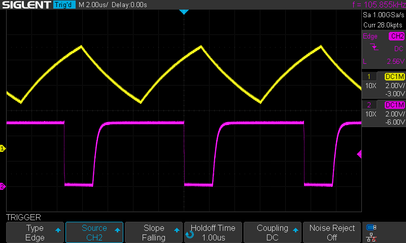
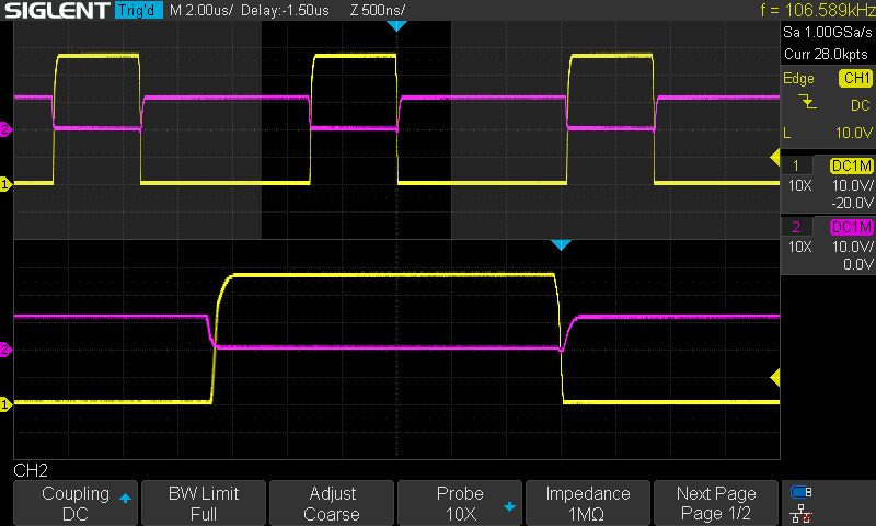
HIN and LIN are in phase and out of phase (respectively) with the PWM signal, and both have their rising edges delayed by about 70 ns. To verify these dead times, let’s look at real-life HIN and LIN through the scope:
Insane ringing! Pardon my humour – I was using those standard-issue 15 cm (6”) ground leads (with crocodile clips) that come with all ‘scopes. I reckon most of the oscillation you see here results from the parasitic inductance of the ground leads, resonating with the probe’s input capacitance in the presence of a fast signal – transition times are just a couple ns here! (For a thorough treatment of such pathologies, I highly recommend AN47 by the late and legendary Jim Williams.)
Output driver & LC filter
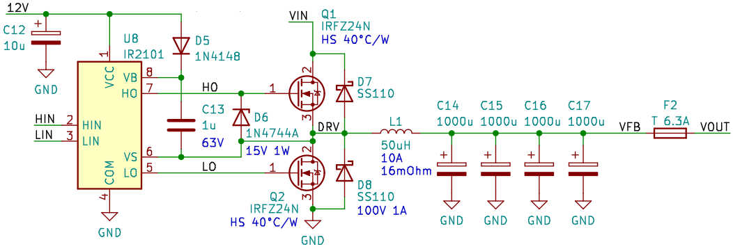
Finally: the actual buck converter! The IR2101 is a dual channel MOSFET driver, with a floating high side driver and a conventional low side driver. The high side drive voltage is bootstrapped via D5 and C13. This is a simple scheme that works well with continuously running switchers such as this one. Periodic low side conduction is required to replenish the bootstrap capacitor C13 via D5; if we wanted to drive the high side switch for a prolonged period, we would need a more sophisticated solution.
The chosen MOSFET (IRFZ24N) has a drain-source breakdown voltage rating of 55V. A bit on the low side, as the 48V battery, completely charged, will be over 50V. However, the pleasantly low total gate charge (20 nC) of this device allows the IR2101 to drive fast transitions. And its low ON-resistance (44 mΩ, or perhaps 70 mΩ depending on manufacturer / datasheet version…) makes it dissipate less than 2 watts at our full current rating, further diluted by the switch duty cycle. A small heatsink (as spec’d) is all we need.
An alternative MOSFET, such as the IRF540, could be substituted for a comfortable 100V drain-source breakdown. The price would be a total gate charge of 70 nC (a 3.5-fold increase!), leading to higher IR2101 supply current draw (boosted by a similar factor) and slower switch transitions.
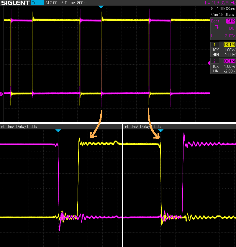
As it stands, the MOSFET gate voltages HO and LO look pretty clean in reality (measured in the lab with a VIN supply voltage of 36V):
In the above trace HO (yellow) and LO (pink) are measured at idle load conditions (I found no significant deterioration with load applied). The vertical offsets of the traces are off by two divs; the bottom of the pink trace should be flush with the bottom of the yellow one. But it’s easy enough to see that referenced to circuit ground, the high side gate drive jumps up several tens of volts (the VIN supply potential of the source terminal plus a 12V gate drive imposed on top, close to 50V in our case) while the low side gate drive jumps 12V only. That is the floating high side driver in action! The bottom split (zooming in on the top split with darkened background) confirms that the IR2101 is doing an excellent job. But even so, transitions are quite visibly far from instantaneous, even with the IRFZ24N’s comparatively low gate charge.
So what’s with the diodes around the switches? D7 and D8 act as protection against potentially harmful transients (anticipated ringing). They are Schottky diodes for the sake of no reverse recovery. The MOSFET integrated body diodes are basically ultra-fast silicon rectifiers. There would be no point in duplicating them in discrete form; any protective effect would be diminished by their reverse recovery times. Schottky diodes, on the other hand, are free from reverse recovery effects.
That leaves us with D6. That is a 15V Zener diode to protect the gate of Q1 from overvoltage (gate-source breakdown, as usual with power MOSFETs, is rated at a mere 20V). I did not anticipate the need for this diode (it was absent from the initial design), until I… shorted the output of the regulator. That left me with a dead Q1, destroyed in an instant by gate-source breakdown. Just look at the yellow trace above to understand why…
I did my part of head scratching, taking deep breaths and thinking. Finally, I soldered this Zener right on top of the MOSFET leads (on the bottom side of the prototype PCB). Several output shorts later, Q1 (the last one soldered in) is still alive and kicking. That’s some strong evidence this Zener really protects the high side switch!
But how did all those output short circuits happen? I’m so glad you asked! Read on…
Overvoltage crowbar
Here’s an Easter egg I haven’t talked about yet.
My goal with this converter was to supply backup power to critical (to me!) computing infrastructure, so I wanted to make it fail in a safe way. That is, I wanted insurance against downstream damage in the event of the regulator developing some fault, or meeting some unforeseen condition, that takes the output voltage appreciably above the nominal 12V.
A simple solution to this problem is hanging an overvoltage crowbar on the output. My circuit is a very direct adaptation from the one published in The Art of Electronics (3rd ed.), pp.691. The crowbar’s task is to put an unrelenting short circuit across the output (therefore blowing the output fuse) in case the output voltage is ever above the threshold.
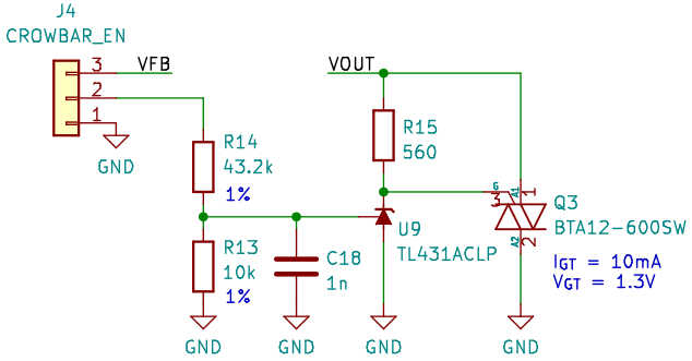
And voila, now I have a TL431 in my circuit! Any time it senses a voltage greater than 2.5V via the voltage divider, it will go into heavy conduction, turning on triac Q3. That will short VOUT to ground, and due to the way triacs work, the short will remain there until VOUT disappears one way or another – it’s a VOUT killer! (We hope the output fuse F2, and only that, will melt.)
Due to the brute-force nature of this circuit add-on, I added a 3-pin jumper header to enable or disable the crowbar depending on where the jumper is placed: a jumper on pins 1-2 will disable it; 2-3 will enable sensing the output voltage.
I think you know where this story is heading, with all the short circuits! And we will soon get to it – but first let me talk about the prototype and some initial measurements.
Prototype construction
As usual, I built some experimental parts of the circuit on a solderless breadboard. But in full recognition of its limitations (not suitable for a combination of fast signals and large currents), I only validated a few details (such as RC component sizing for the 555 oscillator and the dead time generator) instead of the complete circuit.
For the complete prototype, I designed a custom PCB of the usual dual layer type. The soldering side is used as a ground plane with very few intruding routes. The board dimensions are a comfortable and round 80 x 120 mm. I placed several test points to facilitate lab measurements.
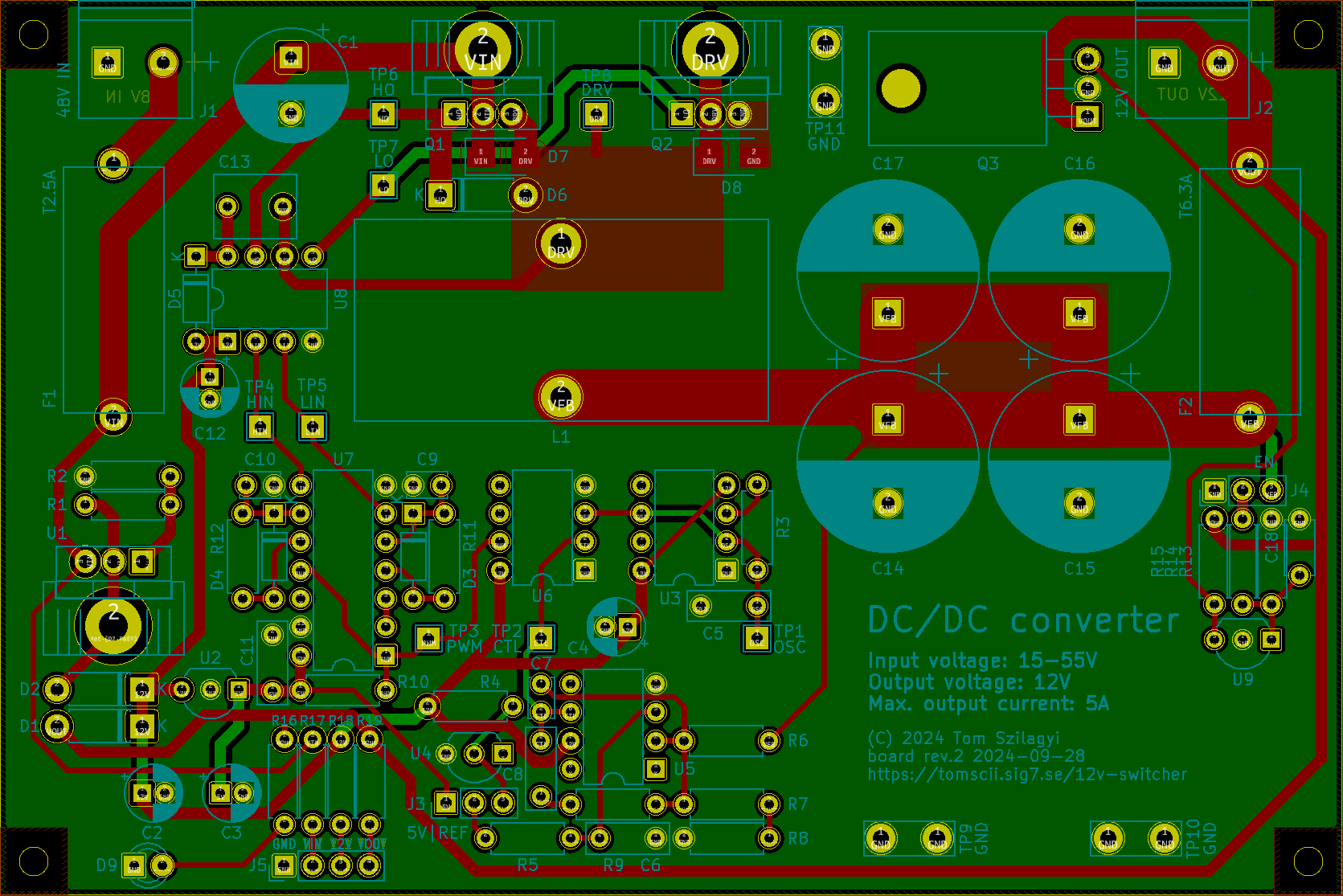
PCB design in KiCAD 6 (click to enlarge)
I used through-hole components (with the sole exception of Schottky diodes D7 and D8) for easy construction and debugging. The capacitors are either electrolytic (the big ones in the LC filter specifically low-ESR types) or polyester (for the smaller filtering/timing caps).
After the obligatory long wait, the PCB finally arrived from the factory and I quickly soldered it all, excited to perform first measurements.
But first thing first – a smoke test verified that to a first approximation, the switcher works! Its output voltage, as measured by my trusty old DMM, read 11.99V. I quite like that number, especially since we are using the 5V regulated supply as reference voltage (I decided to skip the precision shunt regulator on this first prototype). So far so good!
Measurements
This is the very first design aided by my brand new oscilloscope, a Siglent SDS2352X-E digital storage scope with 350 MHz analog bandwidth and 2 GSa/s sampling capability. I have spent too many decades without a proper scope; now I am looking forward to several more decades of blissful measurements!
The below tests were all made connecting the switcher to my laboratory supply set to a moderate to high voltage (24 to 36V).
Slow start
Upon connecting the power supply, the switcher’s output voltage rises thusly:
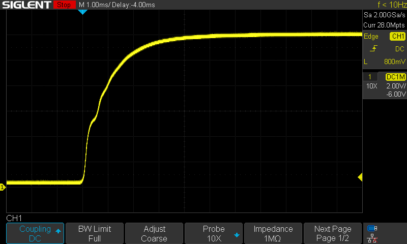
This is an almost perfect replica of the theoretical slow start curve from the time-domain (transient) simulation I presented above! We can even see a similar (but less pronounced) bump, here around half a millisecond into the rise. The exponential curve’s time constant looks the same; no sight of overshoot or instability. I found this encouraging, so proceeded with load testing.
Load testing
For testing the supply with switched loads, I used a little device made earlier from two 2.2 Ω 17W power resistors and two switches, able to turn the load into either a series or parallel connection of these resistors, or only one of them. So we can have load resistances of 4.4 Ω, 2.2 Ω and 1.1 Ω, or an open circuit, depending on the switches.
I also took some length of resistance wire I found, lacking any closer specification, but measured about 8 Ω across its full length of 140 cm. I made an ad-hoc rheostat out of this wire with the help of some bench clamps and crocodile clips. By sliding one of the clips gripping the wire, the resistance can be carefully and gradually altered.
The regulated current was flown through my custom stand-alone current meter (as-of-yet unpublished; built on a perf-board out of a 10 mΩ shunt resistance, some op-amps, a microcontroller and small LCD). Here’s a photo of the whole arrangement:
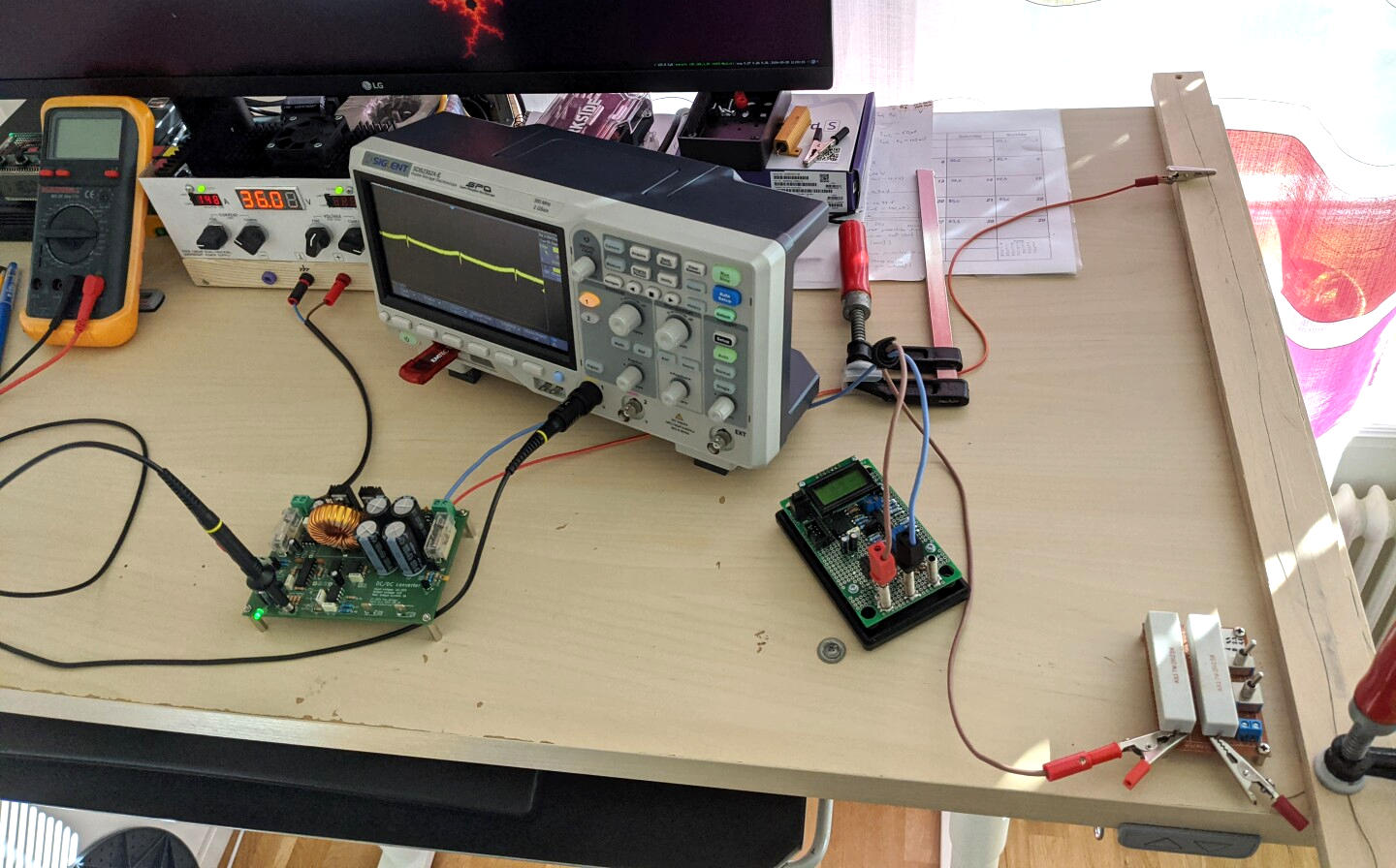
Load testing: PSU & scope; ammeter, power resistors, resistance wire… (click to enlarge)
The output voltage was measured at the switcher’s monitoring output, an unpopulated pin header whose layout conveniently allowed sticking the probe tip, equipped with the low-inductance ground spring contact (instead of the 6” ground lead), just into the right holes.
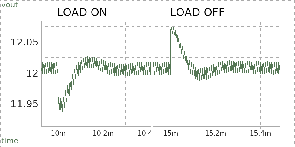
I was, first and foremost, interested in how well the control loop regulates the output voltage in the face of load transients. So I tweaked the total resistance until the ammeter indicated very close to 1A current, and triggered some captures switching this load on and off:
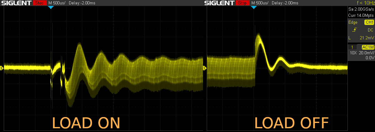
Load transients in reality (click to enlarge)
Here we are looking at an AC-filtered, magnified view (20 mV/div) of the output voltage. Comparing these traces with our immaculate simulation results presented earlier, apparently reality is… uglier. Part of the ugliness is due to some mechanical switch bounce (start of the turn-on). More importantly, it looks like the control loop is not as perfect as it seemed in theory – there is some major ringing around 1.4 kHz, damped but only sub-optimally so. This lengthens the transient settling time, even if its peak amplitude is only about 40 mV. Well, according to our simulations, the compensation network should provide close to maximum phase boost at this frequency, so the system should be far from oscillating.
Finally, it seems the ripple amplitude is heavily dependent on load current! It goes way up (trace widens) with a 1A output current. Our model did not predict anything like that!
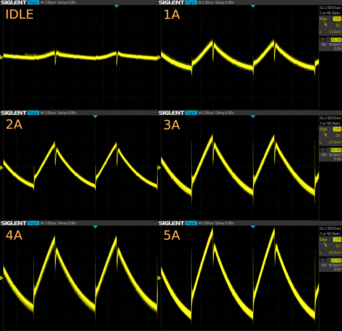
To explore the output ripple at various load levels, I did a series of measurements from idle to the full rated load of 5A, in roughly quarter-amp steps. Throughout this process, I recorded voltage and current readouts of my lab supply (measuring input power) as well as output current from the ammeter, so I could compute the converter’s efficiency. At each step, I also recorded the ripple as displayed on the scope. For brevity, here I only include half-amp steps of current, along with calculated efficiency:
| Iout [A] | Vin [V] | Iin [A] | η [%] |
|---|---|---|---|
| 0.00 | 36.00 | 0.02 | N/A |
| 1.00 | 36.13 | 0.37 | 89.7% |
| 1.50 | 36.00 | 0.54 | 92.6% |
| 2.00 | 36.00 | 0.70 | 95.2% |
| 2.52 | 36.06 | 0.89 | 94.2% |
| 3.01 | 36.00 | 1.06 | 94.7% |
| 3.50 | 36.00 | 1.22 | 95.6% |
| 4.03 | 36.06 | 1.41 | 95.1% |
| 4.50 | 36.00 | 1.59 | 94.3% |
| 5.03 | 36.00 | 1.78 | 94.2% |
Converter efficiency η (the ratio of output power to input power, expressed as a percentage) hovers around 94%, which is excellent! Even if more or less expected due to the synchronous converter topology, it’s still nice to see the design deliver on its promise! During the tests, I regularly checked MOSFET heatsinks with my finger. There was pretty much nothing at 1A; they started to get warm at around 3A and got hot (but not burning hot) at 5A.
So let’s look at those scope traces in detail! I will only show a composite made at whole-amp steps (all traces 2 μs/div horizontal, 10 mV/div vertical):
Output ripple at loads idle to full (click to enlarge)
Why does the ripple amplitude increase so steadily with output current? The textbook model of buck converters does not do this! It took me quite some head scratching to come up with an explanation, but I think I understand now. The LC filter inductance (the nice big toroid) is 50 μH – but only nominally! In reality, the core material (some kind of ferrite powder; I don’t have a datasheet) has a non-constant relative permeability μr, decreasing as the core is magnetized with ever larger currents. That is, equal increases in H will lead to diminishing increases in B as the core’s magnetization moves towards saturation. In practice, the inductance “looks” like it is losing some of its value as we increase its dc bias current.
As a rough estimation, at 5A the voltage ramp is 3.5 times the amplitude at 1A. This ramp reflects the inductor’s current ramp, via the filter capacitance (both the voltage drop on its ESR and the capacitance voltage proportional to stored charge). All else equal, elementary theory leads us to think that a 3.5-fold increase in ripple amplitude is due to an inductance reduction by the same factor! Luckily, even at full load, the 70 mVpp ripple amplitude is acceptable. But I’m sure my next switcher will have a better specified inductor in it, so I can model this effect in advance!
That leaves us with a final question: what are those very sharp spikes that also seem to get larger along with the ripple? Again, some unmodeled second-order effect. My guess is that these substantial transients are due to non-ideal behaviour of the MOSFET switches, fueled by so-called hard switching. I suspect parasitics might also be at play here. (Filter capacitor’s lead inductance? Inductor’s winding capacitance?) It ain’t easy to find textbook treatment of such higher-order effects!
But let’s not despair – our model was simple, computationally cheap, and we still got a working converter as a result, not too bad for a first try! It reached its full output current without batting an eye:
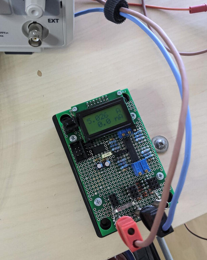
Full load according to ammeter – mission accomplished! (click to enlarge)
Crowbar + small cap = surprise destroyer!
Throughout these adventures, the overvoltage crowbar has been sitting there quietly, enabled but (thankfully) doing nothing. I did not think too much about it; the threshold voltage is designed to be a little over 13V. The output is regulated to 12V with negligible error, and the largest transient is, as demonstrated, well under a tenth of a volt. What could go wrong?
Still thinking about the output ripple, spikes and all, I thought hmm, maybe we need to hang some smaller caps on the output… The large electrolytics are likely less effective at higher frequencies. So as a quick experiment, I took a 100 nF polyester capacitor and shorted it to the output, right to the screw terminal block, while the regulator was running idle.
And… BOOM! My lab supply went red (indicating current limiting). The output got shorted and this killed the high-side MOSFET. (Both fuses in the circuit remained intact, due to the current limit set on the lab supply.) To be honest, I was shocked! Okay, I know circuits can act in surprising ways, but come on… How can a measly little 0.1 μF cap, shorted to an already existing 4000 μF of capacitance, have such a dramatic effect?
But first, I got to the business of swapping in a new MOSFET, and coming up with a way to protect it (eventually adding Zener diode D6 to the circuit, as mentioned above). Then I tried to capture the output transient causing havoc, with the crowbar disabled. Below is a capture of VOUT during the very same action (500 ns/div horizontal, 500 mV/div vertical):
![]()
I admit, the amplitude is bigger than I anticipated, but still below the crowbar threshold. Plus, the frequency of this ringing is about 2 MHz and it decays in a few μs – how on Earth does it trigger the crowbar’s input, given the RC time constant of close to ten μs (from the Thevenin-equivalent of the voltage divider R14-R13, and the 1 nF filter capacitor C18)?
I have no idea, but maybe brute force helps. I increased the filter to 10 nF. Re-armed the crowbar. Shorted the 100 nF “killer cap” (with trembling hands). Nothing! Oh, phew, okay, guess we are good. Let’s try a 1 μF cap then, shall we? Must surely withstand that, too?
BOOM! Supply into the red. This is not good! But this time, the MOSFET survived!
As a quick experiment, I inserted a 10 μH choke into the path to the voltage divider (in place of the jumper). With the upgraded “killer cap” of 1 μF, the problem persisted.
Hmm, maybe the voltage divider’s output is a bit too close to the actual threshold of the TL431… I changed the 43.2k upper leg of the divider to 47k, for an increase of threshold voltage from 13.1V to 14.2V. Did it matter? Absolutely not!
I was starting to get a little desperate. I increased the filter cap to a ridiculous 100 nF. It did not help. Added 10 nF directly across legs 2 and 3 of the triac Q3. Still the same. Added 1 nF directly across the TL431 input and its ground (on the PCB bottom). Nope, still nope.
I thought it was time to give up on the crowbar, but then I got another idea. Let’s try to shorten the inductive sensing path! I cut the component-side PCB trace to the right of J4 (originally connecting it to a VOUT track) and connected the rightmost pin directly to the F2 fuse holder’s lead with a short wire (underside the PCB), labeled VFB. That way the crowbar’s sensing voltage is sourced from the storage caps more or less directly, without going around in a lengthy loop with the output terminal along the path. I also made this change on the PCB design, as it seemed like such a clever move. And I was pretty confident that I got to the bottom of the issue…
Did it solve the problem? Absolutely not! The only good news was that the high-side MOSFET survived through at least half a dozen output short circuits. If nothing else, at least the Zener protection works fine!
My vague theory: the actual crowbar-triggering spike is not what I was able to measure. Rather, the real spike is inductively coupled to the input of the TL431. Hence, it does not go through the voltage divider and transient filter at all (so neither a raised threshold, nor an increased time constant poses any obstacle). I am at a loss trying to explain why my last fix attempt did not work; it seems like a more thorough understanding and a redesigned PCB layout might be necessary to fully eliminate this issue.
For the moment, the output crowbar stays disabled. The rest of the circuit gets a pass. So does my lab supply – repeatedly proven itself against rogue loads, and the current limiting feature is a life saver!
The End… for now!
Switch-mode power conversion is, in theory, a simple and elegant concept. In practice… well, as I found out, there be dragons! I have barely scratched the surface of what there is to know, but still, it feels like I made some headway into this terra incognita.
That said, I am not exactly done with this project, but this article is too long already! So even though more research is definitely needed, I now have a switcher that seems to work, and I will stop here. Possible improvements I would like to try, some time or another:
tune the control loopimprove the compensator;- use a better inductance;
- add an additional LC output filter to reduce ripple;
- make the crowbar safely usable.
If you have read so far and have any thoughts on this project, feel free to contact me. And if you are an experienced electronics engineer and have some advice or guidance on what I am doing wrong (or could do even better), I would love to hear from you!
As always, the sources of this article (in this case, the KiCAD hardware design plus XSchem workspaces and ngspice simulation files) are published online with everything licensed under the terms of the very permissive MIT license.